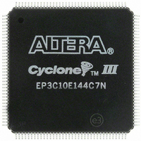
EP3C10E144C7N Altera, EP3C10E144C7N Datasheet - Page 6

EP3C10E144C7N
Manufacturer Part Number
EP3C10E144C7N
Description
IC CYCLONE III FPGA 10K 144-EQFP
Manufacturer
Altera
Series
Cyclone® IIIr
Datasheets
1.EP3C5F256C8N.pdf
(5 pages)
2.EP3C5F256C8N.pdf
(34 pages)
3.EP3C5F256C8N.pdf
(66 pages)
4.EP3C5F256C8N.pdf
(14 pages)
5.EP3C5F256C8N.pdf
(76 pages)
Specifications of EP3C10E144C7N
Number Of Logic Elements/cells
10320
Number Of Labs/clbs
645
Total Ram Bits
423936
Number Of I /o
94
Voltage - Supply
1.15 V ~ 1.25 V
Mounting Type
Surface Mount
Operating Temperature
0°C ~ 85°C
Package / Case
144-EQFP
For Use With
544-2601 - KIT DEV CYCLONE III LS EP3CLS200544-2411 - KIT DEV NIOS II CYCLONE III ED.
Lead Free Status / RoHS Status
Lead free / RoHS Compliant
Number Of Gates
-
Other names
544-2425
EP3C10E144C7N
EP3C10E144C7N
Available stocks
Company
Part Number
Manufacturer
Quantity
Price
Company:
Part Number:
EP3C10E144C7N
Manufacturer:
ALTERA
Quantity:
364
Part Number:
EP3C10E144C7N
Manufacturer:
ALTERA
Quantity:
20 000
1–6
Cyclone III Device Family Architecture
Logic Elements and Logic Array Blocks
Memory Blocks
Cyclone III Device Handbook, Volume 1
f
Table 1–5
Table 1–5. Cyclone III Device Family Configuration Schemes
Cyclone III device family includes a customer-defined feature set that is optimized for
portable applications and offers a wide range of density, memory, embedded
multiplier, and I/O options. Cyclone III device family supports numerous external
memory interfaces and I/O protocols that are common in high-volume applications.
The Quartus II software features and parameterizable IP cores make it easier for you
to use the Cyclone III device family interfaces and protocols.
The following sections provide an overview of the Cyclone III device family features.
The logic array block (LAB) consists of 16 logic elements and a LAB-wide control
block. An LE is the smallest unit of logic in the Cyclone III device family architecture.
Each LE has four inputs, a four-input look-up table (LUT), a register, and output logic.
The four-input LUT is a function generator that can implement any function with four
variables.
For more information about LEs and LABs, refer to the
Blocks in Cyclone III Devices
Each M9K memory block of the Cyclone III device family provides nine Kbits of
on-chip memory capable of operating at up to 315 MHz for Cyclone III devices and up
to 274 MHz for Cyclone III LS devices. The embedded memory structure consists of
M9K memory blocks columns that you can configure as RAM, first-in first-out (FIFO)
buffers, or ROM. The Cyclone III device family memory blocks are optimized for
applications such as high throughout packet processing, embedded processor
program, and embedded data storage.
The Quartus II software allows you to take advantage of the M9K memory blocks by
instantiating memory using a dedicated megafunction wizard or by inferring memory
directly from the VHDL or Verilog source code.
M9K memory blocks support single-port, simple dual-port, and true dual-port
operation modes. Single-port mode and simple dual-port mode are supported for all
port widths with a configuration of ×1, ×2, ×4, ×8, ×9, ×16, ×18, ×32, and ×36. True
dual-port is supported in port widths with a configuration of ×1, ×2, ×4, ×8, ×9, ×16,
and ×18.
lists Cyclone III device family configuration schemes.
Joint Test Action Group (JTAG)
Fast passive parallel (FPP)
Configuration Scheme
Active parallel (AP)
Passive serial (PS)
Active serial (AS)
chapter.
Chapter 1: Cyclone III Device Family Overview
Cyclone III
Logic Elements and Logic Array
v
v
v
v
v
© December 2009 Altera Corporation
Cyclone III Device Family Architecture
Cyclone III LS
v
—
v
v
v


