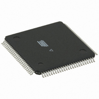
AT40K05AL-1AQC Atmel, AT40K05AL-1AQC Datasheet - Page 27

AT40K05AL-1AQC
Manufacturer Part Number
AT40K05AL-1AQC
Description
IC FPGA 5K GATES 100TQFP
Manufacturer
Atmel
Series
AT40KALr
Specifications of AT40K05AL-1AQC
Number Of Logic Elements/cells
256
Total Ram Bits
2048
Number Of I /o
78
Number Of Gates
10000
Voltage - Supply
3 V ~ 3.6 V
Mounting Type
Surface Mount
Operating Temperature
0°C ~ 70°C
Package / Case
100-TFQFP
Lead Free Status / RoHS Status
Contains lead / RoHS non-compliant
Number Of Labs/clbs
-
Available stocks
Company
Part Number
Manufacturer
Quantity
Price
Company:
Part Number:
AT40K05AL-1AQC
Manufacturer:
ATMEL
Quantity:
460
AC Timing Characteristics – 3.3V Operation
Delays are based on fixed loads and are described in the notes.
Maximum times based on worst case: V
Minimum times based on best case: V
Maximum delays are the average of t
Clocks and Reset Input buffers are measured from a V
Maximum times for clock input buffers and internal drivers are measured for rising edge delays only.
2818F–FPGA–07/06
Cell Function
Global Clocks and Set/Reset
GCLK Input Buffer
FCLK Input Buffer
Clock Column Driver
Clock Sector Driver
GSRN Input Buffer
Global Clock to Output
Fast Clock to Output
Parameter
t
(Maximum)
t
(Maximum)
t
(Maximum)
t
(Maximum)
t
(Maximum)
t
(Maximum)
t
(Maximum)
PD
PD
PD
PD
PD
PD
PD
PDLH
CC
CC
= 3.6V, temperature = 0°C
and t
= 3.0V, temperature = 70°C
Path
pad -> clock
pad -> clock
pad -> clock
pad -> clock
pad -> clock
pad -> clock
pad -> clock
pad -> clock
clock -> colclk
clock -> colclk
clock -> colclk
clock -> colclk
colclk -> secclk
colclk -> secclk
colclk -> secclk
colclk -> secclk
pad -> GSRN
pad -> GSRN
pad -> GSRN
pad -> GSRN
clock pad -> out
clock pad -> out
clock pad -> out
clock pad -> out
clock pad -> out
clock pad -> out
clock pad -> out
clock pad -> out
PDHL
.
IH
of 1.5V at the input pad to the internal V
Device
AT40K05AL
AT40K10AL
AT40K20AL
AT40K40AL
AT40K05AL
AT40K10AL
AT40K20AL
AT40K40AL
AT40K05AL
AT40K10AL
AT40K20AL
AT40K40AL
AT40K05AL
AT40K10AL
AT40K20AL
AT40K40AL
AT40K05AL
AT40K10AL
AT40K20AL
AT40K40AL
AT40K05AL
AT40K10AL
AT40K20AL
AT40K40AL
AT40K05AL
AT40K10AL
AT40K20AL
AT40K40AL
AT40KAL Series FPGA
1.1
1.2
1.2
1.4
0.7
0.8
0.8
0.8
0.8
0.9
1.0
1.1
0.5
0.5
0.5
0.5
3.0
3.7
4.3
5.6
8.3
8.4
8.6
8.8
7.9
8.0
8.1
8.3
-1
Units
ns
ns
ns
ns
ns
ns
ns
ns
ns
ns
ns
ns
ns
ns
ns
ns
ns
ns
ns
ns
ns
ns
ns
ns
ns
ns
ns
ns
Notes
Rising edge clock
Rising edge clock
Rising edge clock
Rising edge clock
From any pad to Global
Set/Reset network
Rising edge clock
Fully loaded clock tree
Rising edge DFF
20 mA output buffer
50 pf pin load
Rising edge clock
Fully loaded clock tree
Rising edge DFF
20 mA output buffer
50 pf pin load
IH
of 50% of V
CC
.
27


