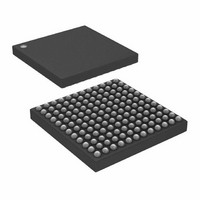
ADSP-2184NKCA-320 Analog Devices Inc, ADSP-2184NKCA-320 Datasheet - Page 8

ADSP-2184NKCA-320
Manufacturer Part Number
ADSP-2184NKCA-320
Description
IC DSP 16BIT 80MHZ 144CSPBGA
Manufacturer
Analog Devices Inc
Series
ADSP-21xxr
Type
Fixed Pointr
Datasheet
1.ADSP-2185NKSTZ-320.pdf
(48 pages)
Specifications of ADSP-2184NKCA-320
Rohs Status
RoHS non-compliant
Interface
Host Interface, Serial Port
Clock Rate
80MHz
Non-volatile Memory
External
On-chip Ram
20kB
Voltage - I/o
3.30V
Voltage - Core
1.80V
Operating Temperature
0°C ~ 70°C
Mounting Type
Surface Mount
Package / Case
144-CSPBGA
Device Core Size
16b
Architecture
Enhanced Harvard
Format
Fixed Point
Clock Freq (max)
80MHz
Mips
80
Device Input Clock Speed
80MHz
Ram Size
20KB
Program Memory Size
Not RequiredKB
Operating Supply Voltage (typ)
1.8/2.5/3.3V
Operating Supply Voltage (min)
1.71V
Operating Supply Voltage (max)
1.89/3.6V
Operating Temp Range
0C to 70C
Operating Temperature Classification
Commercial
Mounting
Surface Mount
Pin Count
144
Package Type
CSPBGA
Package
144CSP-BGA
Numeric And Arithmetic Format
Fixed-Point
Maximum Speed
80 MHz
Device Million Instructions Per Second
80 MIPS
Lead Free Status / Rohs Status
Not Compliant
Available stocks
Company
Part Number
Manufacturer
Quantity
Price
Company:
Part Number:
ADSP-2184NKCA-320
Manufacturer:
Analog Devices Inc
Quantity:
10 000
ADSP-218xN
Clock Signals
ADSP-218xN series members can be clocked by either a crystal
or a TTL-compatible clock signal.
The CLKIN input cannot be halted, changed during operation,
nor operated below the specified frequency during normal oper-
ation. The only exception is while the processor is in the power-
down state. For additional information, refer to the ADSP-218x
DSP Hardware Reference, for detailed information on this
power-down feature.
If an external clock is used, it should be a TTL-compatible signal
running at half the instruction rate. The signal is connected to
the processor’s CLKIN input. When an external clock is used,
the XTAL pin must be left unconnected.
ADSP-218xN series members use an input clock with a fre-
quency equal to half the instruction rate; a 40 MHz input clock
yields a 12.5 ns processor cycle (which is equivalent to
80 MHz). Normally, instructions are executed in a single pro-
cessor cycle. All device timing is relative to the internal instruc-
tion clock rate, which is indicated by the CLKOUT signal
when enabled.
Because ADSP-218xN series members include an on-chip oscil-
lator circuit, an external crystal may be used. The crystal should
be connected across the CLKIN and XTAL pins, with two
capacitors connected as shown in
dependent on crystal type and should be specified by the crystal
manufacturer. A parallel-resonant, fundamental frequency,
microprocessor-grade crystal should be used. To provide an
adequate feedback path around the internal amplifier circuit,
place a resistor in parallel with the circuit, as shown in
A clock output (CLKOUT) signal is generated by the processor
at the processor’s cycle rate. This can be enabled and disabled by
the CLKODIS bit in the SPORT0 Autobuffer Control Register.
RESET
The RESET signal initiates a master reset of the ADSP-218xN.
The RESET signal must be asserted during the power-up
sequence to assure proper initialization. RESET during initial
power-up must be held long enough to allow the internal clock
to stabilize. If RESET is activated any time after power-up, the
clock continues to run and does not require stabilization time.
The power-up sequence is defined as the total time required for
the crystal oscillator circuit to stabilize after a valid V
applied to the processor, and for the internal phase-locked loop
(PLL) to lock onto the specific crystal frequency. A minimum of
Figure 3. External Crystal Connections
C L K IN
D S P
1 M
X T A L
Figure
C L K O U T
3. Capacitor values are
Rev. A | Page 8 of 48 | August 2006
DD
Figure
is
3.
2000 CLKIN cycles ensures that the PLL has locked, but does
not include the crystal oscillator start-up time. During this
power-up sequence the RESET signal should be held low. On
any subsequent resets, the RESET signal must meet the mini-
mum pulse-width specification (t
The RESET input contains some hysteresis; however, if an RC
circuit is used to generate the RESET signal, the use of an exter-
nal Schmitt trigger is recommended.
The master reset sets all internal stack pointers to the empty
stack condition, masks all interrupts, and clears the MSTAT
register. When RESET is released, if there is no pending bus
request and the chip is configured for booting, the boot-loading
sequence is performed. The first instruction is fetched from on-
chip program memory location 0x0000 once boot loading
completes.
POWER SUPPLIES
ADSP-218xN series members have separate power supply con-
nections for the internal (V
supplies. The internal supply must meet the 1.8 V requirement.
The external supply can be connected to a 1.8 V, 2.5 V, or 3.3 V
supply. All external supply pins must be connected to the same
supply. All input and I/O pins can tolerate input voltages up to
3.6 V, regardless of the external supply voltage. This feature pro-
vides maximum flexibility in mixing 1.8 V, 2.5 V, or 3.3 V
components.
DDINT
) and external (V
RSP
).
DDEXT
) power


