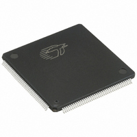
CY37128VP160-83AXC Cypress Semiconductor Corp, CY37128VP160-83AXC Datasheet - Page 17

CY37128VP160-83AXC
Manufacturer Part Number
CY37128VP160-83AXC
Description
IC CPLD 128 MACROCELL 160LQFP
Manufacturer
Cypress Semiconductor Corp
Series
Ultra37000™r
Specifications of CY37128VP160-83AXC
Programmable Type
In-System Reprogrammable™ (ISR™) CMOS
Delay Time Tpd(1) Max
15.0ns
Voltage Supply - Internal
3 V ~ 3.6 V
Number Of Macrocells
128
Number Of I /o
133
Operating Temperature
0°C ~ 70°C
Mounting Type
Surface Mount
Package / Case
160-LQFP
Voltage
3.3V
Memory Type
CMOS
Family Name
Ultra 37000
# Macrocells
128
Number Of Usable Gates
3800
Frequency (max)
83MHz
Propagation Delay Time
15ns
Number Of Logic Blocks/elements
8
# I/os (max)
133
Operating Supply Voltage (typ)
3.3V
In System Programmable
Yes
Operating Supply Voltage (min)
3V
Operating Supply Voltage (max)
3.6V
Operating Temp Range
0C to 70C
Operating Temperature Classification
Commercial
Mounting
Surface Mount
Pin Count
160
Package Type
TQFP
Lead Free Status / RoHS Status
Lead free / RoHS Compliant
Features
-
Number Of Logic Elements/cells
-
Lead Free Status / Rohs Status
Compliant
Available stocks
Company
Part Number
Manufacturer
Quantity
Price
Company:
Part Number:
CY37128VP160-83AXC
Manufacturer:
Cypress Semiconductor Corp
Quantity:
10 000
Company:
Part Number:
CY37128VP160-83AXCT
Manufacturer:
Cypress Semiconductor Corp
Quantity:
10 000
Switching Characteristics
Document Number : 38-03007 Rev. *G
Product Term Clocking Parameters
t
t
t
t
t
t
Pipelined Mode Parameters
t
Operating Frequency Parameters
f
f
f
f
Reset/Preset Parameters
t
t
t
t
t
t
User Option Parameters
t
t
t
t
t
t
f
Notes
COPT
SPT
HPT
ISPT
IHPT
CO2PT
ICS
MAX1
MAX2
MAX3
MAX4
RW
RR
RO
PW
PR
PO
LP
SLEW
3.3IO
S JTAG
H JTAG
CO JTAG
JTAG
11. t
12. All AC parameters are measured with two outputs switching and 35 pF AC Test Load.
13. Logic blocks operating in low power mode, add t
14. Outputs using Slow Output Slew Rate, add t
15. When V
JTAG Timing Parameters
[13]
[13]
[13, 14, 15]
[13, 14, 15]
[13]
ER
[13]
Parameter
[13, 14, 15]
measured with 5 pF AC Test Load and t
[13, 14, 15]
CCO
= 3.3V, add t
Product Term Clock or Latch Enable (PTCLK) to Output
Set-Up Time from Input to Product Term Clock or Latch Enable (PTCLK)
Register or Latch Data Hold Time
Set-Up Time for Buried Register used as an Input Register from Input to Product Term Clock or
Latch Enable (PTCLK)
Buried Register Used as an Input Register or Latch Data Hold Time
Product Term Clock or Latch Enable (PTCLK) to Output Delay (Through Logic Array)
Input Register Synchronous Clock (CLK
Clock (CLK
Maximum Frequency with Internal Feedback (Lesser of 1/t
Maximum Frequency Data Path in Output Registered/Latched Mode (Lesser of 1/(t
1/(t
Maximum Frequency with External Feedback (Lesser of 1/(t
Maximum Frequency in Pipelined Mode (Lesser of 1/(t
or 1/t
Asynchronous Reset Width
Asynchronous Reset Recovery Time
Asynchronous Reset to Output
Asynchronous Preset Width
Asynchronous Preset Recovery Time
Asynchronous Preset to Output
Low Power Adder
Slow Output Slew Rate Adder
3.3V I/O Mode Timing Adder
Set-up Time from TDI and TMS to TCK
Hold Time on TDI and TMS
Falling Edge of TCK to TDO
Maximum JTAG Tap Controller Frequency
3.3IO
S
+ t
SCS
to this specification.
H
)
), or 1/t
[5]
0
, CLK
Over the Operating Range (continued)
EA
CO
SLEW
1
measured with 35 pF AC Test Load.
)
, CLK
[5]
LP
to this specification.
to this specification.
2
, or CLK
[5]
[5]
[5]
[5]
[5]
3
)
[5]
[5]
[5]
0
, CLK
[5]
Description
1
, CLK
2
, or CLK
[12]
CO
+ t
SCS
CO
IS
), 1/t
, 1/(t
3
+ t
) to Output Register Synchronous
S
ICS
S
) or 1/(t
+ t
Ultra37000 CPLD Family
, 1/(t
H
), or 1/t
WL
WL
+ t
+ t
CO
WH
WH
)
WL
[5]
), 1/(t
)
[5]
+ t
IS
WH
+ t
),
IH
),
Page 17 of 43
MHz
MHz
MHz
MHz
Unit
ns
ns
ns
ns
ns
ns
ns
ns
ns
ns
ns
ns
ns
ns
ns
ns
ns
ns
ns
ns
[+] Feedback


