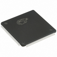
CY7C375I-66AC Cypress Semiconductor Corp, CY7C375I-66AC Datasheet

CY7C375I-66AC
Specifications of CY7C375I-66AC
Related parts for CY7C375I-66AC
CY7C375I-66AC Summary of contents
Page 1
... UltraLogic™ 128-Macrocell Flash CPLD • 3.3V or 5.0V I/O operation • Available in 160-pin TQFP, CQFP, and PGA packages Functional Description The CY7C375i is an In-System Reprogrammable Complex Programmable Logic Device (CPLD) and is part of the F 370i™ family of high-density, high-speed CPLDs. Like LASH ...
Page 2
... CCIO 40 Document #: 38-03029 Rev. *A Top View TQFP CY7C375i V 120 CCIO I/O 119 111 118 I/O 110 117 I/O 109 116 I/O /SDI 108 I/O 115 107 I/O 114 106 113 I/O 105 112 I/O 104 111 GND ...
Page 3
... Document #: 38-03029 Rev. *A Top View CQFP CY7C375i 120 V CC 119 I/O 111 118 I/O 110 117 I/O 109 I/O /SDI 116 108 I/O 115 107 I/O 114 106 I/O 113 105 I/O 112 104 111 GND 110 ...
Page 4
... Like all members of the F 370i family, the CY7C375i is rich LASH in I/O resources. Every macrocell in the device features an associated I/O pin, resulting in 128 I/O pins on the CY7C375i. In addition, there is one dedicated input and four input/clock pins. Finally, the CY7C375i features a very simple timing model. ...
Page 5
... I/O pin is used as an input. Programmable Interconnect Matrix The Programmable Interconnect Matrix (PIM) connects the eight logic blocks on the CY7C375i to the inputs and to each other. All inputs (including feedbacks) travel through the PIM. There is no speed penalty incurred by signals traversing the PIM ...
Page 6
... Max. CC Test Conditions V = 5.0V at f=1 MHz 5. MHz CCINT pin Max. EN CY7C375i Ambient Temperature CCINT 5V ± 0.25V 5V ± 0.25V or 0°C to +70°C 3.3V ± 0.3V −40°C to +85°C 5V ± 0.5V 5V ± 0.5V or 3.3V ± 0.3V –55°C to +125°C 5V ± 0.5V Min ...
Page 7
... JIG AND (b) SCOPE 2.08V(COM'L) 2.13V(MIL) V Output Waveforms--Measurement Level X 1. 0.5V 2.6V 0. 1.5V 0. the V X 0.5V (d) Test Waveforms measured with 35-pF AC Test Load. EA CY7C375i 160-Lead 160-Pin 160-Pin TQFP CQFP CPGA Max. 100 ALL INPUT PULSES 3.0V 90% 10% GND <2ns Unit nH Unit ...
Page 8
... All AC parameters are measured with 16 outputs switching and 35-pF AC Test Load. 14. This specification is intended to guarantee interface compatibility of the other members of the CY7C370i family with the CY7C375i. This specification is met for the devices operating at the same ambient temperature and at the same power supply voltage. ...
Page 9
... Document #: 38-03029 Rev. *A [13] 7C375i–125 7C375i–100 Min. Max. Min. 8 125 100 , 1/( ICS WL WH [9] 10 [9] 12 [1] 16 [9] 10 [9] 12 [1] 16 500 500 CY7C375i 7C375i–83 7C375i–66 7C374iL–83 7C375iL–66 Max. Min. Max. Min 83.3 66 500 500 Max. Unit ...
Page 10
... Switching Waveforms (continued) Latched Output INPUT LATCH ENABLE LATCHED OUTPUT Registered Input REGISTERED INPUT INPUT REGISTER CLOCK COMBINATORIAL OUTPUT CLOCK Clock to Clock REGISTERED INPUT INPUT REGISTER CLOCK OUTPUT REGISTER CLOCK Document #: 38-03029 Rev PDL ICS CY7C375i ICO SCS Page ...
Page 11
... Switching Waveforms (continued) Latched Input LATCHED INPUT LATCH ENABLE COMBINATORIAL OUTPUT LATCH ENABLE Latched Input and Output LATCHED INPUT LATCHED OUTPUT INPUT LATCH ENABLE OUTPUT LATCH ENABLE LATCH ENABLE Document #: 38-03029 Rev PDL ICOL t ICS t WH CY7C375i t ICO PDLL Page ...
Page 12
... CLOCK Output Enable/Disable INPUT OUTPUTS Ordering Information Speed (MHz) Ordering Code 125 CY7C375i–125AC 100 CY7C375i–100AC CY7C375i–100AI 83 CY7C375i–83AC CY7C375i–83AI CY7C375i–83GMB CY7C375i–83UMB CY7C375iL–83AC Document #: 38-03029 Rev Package Name Package Type A160 160-Lead Thin Quad Flatpack ...
Page 13
... Ordering Information (continued) Speed (MHz) Ordering Code 66 CY7C375i–66AC CY7C375i–66AI CY7C375i–66GMB CY7C375i–66UMB CY7C375iL–66AC MILITARY SPECIFICATIONS Group A Subgroup Testing DC Characteristics Parameter Switching Characteristics Parameter 10, 11 ICO 10, 11 ICS Note: 15. Standard product ships trim and formed in a carrier. This product is also available in a molded carrier ring. Contact local Cypress office for package information. ...
Page 14
... Package Diagrams 160-Pin Thin Plastic Quad Flat Pack ( 1.4 mm)(TQFP) A160 Document #: 38-03029 Rev. *A CY7C375i 51-85049-*B Page ...
Page 15
... Package Diagrams (continued) Document #: 38-03029 Rev. *A 160-Pin PGA G160 CY7C375i 51-80012-*A Page ...
Page 16
... SQ. 31.20 ±0.25 (1.228 ±.010) SQ. SEE DETAIL A 0.15 ±0.02 (.006 ±.001) 0.51 ±0.20 (.020 ±.008) CY7C375i DIMENSION IN MM (INCH) REFERENCE JEDEC: N/A PKG. WEIGHT: 6-7gms R 0.13(.005) MIN. 0°-7° 0.20 MIN. (.008 MIN.) 0° MIN. ...
Page 17
... Document History Page Document Title: CY7C375i UltraLogic™ 128-Macrocell Flash CPLD Document Number: 38-03029 REV. ECN NO. Issue Date ** 106374 09/15/01 *A 213375 See ECN Document #: 38-03029 Rev. *A Orig. of Change SZV Change from Spec number: 38-00494 to 38-03029 FSG Added note to title page: “Use Ultra37000 For All New Designs” ...


