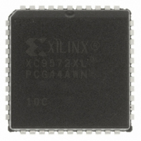
XC9572XL-10PCG44C Xilinx Inc, XC9572XL-10PCG44C Datasheet - Page 4
XC9572XL-10PCG44C
Manufacturer Part Number
XC9572XL-10PCG44C
Description
IC CPLD 72 MCELL C-TEMP 44-PLCC
Manufacturer
Xilinx Inc
Series
XC9500XLr
Specifications of XC9572XL-10PCG44C
Programmable Type
In System Programmable (min 10K program/erase cycles)
Delay Time Tpd(1) Max
10.0ns
Voltage Supply - Internal
3 V ~ 3.6 V
Number Of Logic Elements/blocks
4
Number Of Macrocells
72
Number Of Gates
1600
Number Of I /o
34
Operating Temperature
0°C ~ 70°C
Mounting Type
Surface Mount
Package / Case
44-PLCC
Voltage
3.3V
Memory Type
FLASH
Cpld Type
FLASH
No. Of Macrocells
72
No. Of I/o's
34
Propagation Delay
10ns
Global Clock Setup Time
6.5ns
Frequency
100MHz
Supply Voltage Range
3V To 3.6V
Operating
RoHS Compliant
Lead Free Status / RoHS Status
Lead free / RoHS Compliant
For Use With
122-1512 - KIT DESIGN CPLD W/BATT HOLDER
Features
-
Number Of Logic Elements/cells
-
Lead Free Status / RoHS Status
Lead free / RoHS Compliant
Other names
122-1466
Available stocks
Company
Part Number
Manufacturer
Quantity
Price
Company:

Part Number:
XC9572XL-10PCG44C
Manufacturer:
XILINX
Quantity:
1 200
Company:
Part Number:
XC9572XL-10PCG44C
Manufacturer:
XILINX
Quantity:
220
Company:
Part Number:
XC9572XL-10PCG44C
Manufacturer:
Xilinx Inc
Quantity:
10 000
Part Number:
XC9572XL-10PCG44C
Manufacturer:
XILINX/赛灵思
Quantity:
20 000


XA9500XL Automotive CPLD Product Family
7. Do not drive I/Os pins above the V
8. Do not rely on the I/O states before the CPLD
9. Use a voltage regulator which can provide sufficient
10. Ensure external JTAG terminations for TMS, TCK, TDI,
11. Attach all CPLD V
12. Decouple all V
Recommendations
The following recommendations are for all automotive appli-
cations.
1. Use strict synchronous design (only one clocking event)
2. Include JTAG stakes on the PCB. JTAG stakes can be
4
I/O bank.
a. The current flow can go into V
b. It can also increase undesired leakage current
c. If done for too long, it can reduce the life of the
configures.
current during device power up. As a rule of thumb, the
regulator needs to provide at least three times the peak
current while powering up a CPLD in order to guarantee
the CPLD can configure successfully.
TDO comply with IEEE 1149.1. All Xilinx CPLDs have
internal weak pull-ups of ~50 kΩ on TDI, TMS, and
TCK.
necessary power and ground supplies around the
CPLD.
0.01 μF and 0.1 μF closest to the pins for each
V
if possible. A synchronous system is more robust than
an asynchronous one.
used to test the part on the PCB. They add benefit in
CC
voltage regulator.
associated with the device.
device.
/V
CCIO
-GND pair.
CC
and V
CC
and GND pins in order to have
CCIO
pins with capacitors of
CCIO
CCIO
and affect a user
assigned to its
www.xilinx.com
3. XA9500XL Automotive CPLDs work with any power
4. Do not disregard report file warnings. Software
5. Understand the Timing Report. This report file provides
6. Review Fitter Report equations. Equations can be
7. Let design software define pinouts if possible. Xilinx
8. Perform a post-fit simulation for all speeds to identify
9. Distribute SSOs (Simultaneously Switching Outputs)
10. Terminate high speed outputs to eliminate noise caused
reprogramming part on the PCB, inspecting chip
internals with INTEST, identifying stuck pins, and
inspecting programming patterns (if not secured).
sequence, but it is preferable to power the V
(internal V
which any glitches from device I/Os are unwanted.
identifies potential problems when compiling, so the
report file is worth inspecting to see exactly how your
design is mapped onto the logic.
a speed summary along with warnings. Read the timing
file (*.tim) carefully. Analyze key signal chains to
determine limits to given clock(s) based on logic
analysis.
shown in ABEL-like format, or can also be displayed in
Verilog or VHDL formats. The Fitter Report also
includes switch settings that are very informative of
other device behaviors.
CPLD software works best when it selects the I/O pins
and manages resources for users. It can spread signals
around and improve pin-locking. If users must define
pins, plan resources in advance.
any possible problems (such as race conditions) that
might occur when fast-speed silicon is used instead of
slow-speed silicon.
evenly around the CPLD to reduce switching noise.
by very fast rising/falling edges.
CC
) before the V
CCIO
DS108-1 (v1.7) April 3, 2007
for the applications in
Product Specification
CCI
R
Related parts for XC9572XL-10PCG44C
Image
Part Number
Description
Manufacturer
Datasheet
Request
R

Part Number:
Description:
IC CPLD 72 MCELL C-TEMP 44-PLCC
Manufacturer:
Xilinx Inc
Datasheet:

Part Number:
Description:
IC CPLD 72 MCELL C-TEMP 44-VQFP
Manufacturer:
Xilinx Inc
Datasheet:
Part Number:
Description:
IC CPLD 72 MCELL C-TEMP 64-VQFP
Manufacturer:
Xilinx Inc
Datasheet:

Part Number:
Description:
IC CPLD 72 MCELL C-TEMP 100-TQFP
Manufacturer:
Xilinx Inc
Datasheet:
Part Number:
Description:
IC CPLD 72 MCELL C-TEMP 44-PLCC
Manufacturer:
Xilinx Inc
Datasheet:
Part Number:
Description:
IC CPLD 72 MCELL C-TEMP 100-TQFP
Manufacturer:
Xilinx Inc
Datasheet:
Part Number:
Description:
IC CPLD 72 MCELL C-TEMP 44-PLCC
Manufacturer:
Xilinx Inc
Datasheet:
Part Number:
Description:
IC CPLD 72 MCELL C-TEMP 44-VQFP
Manufacturer:
Xilinx Inc
Datasheet:

Part Number:
Description:
IC CPLD 72MCRCELL 10NS 44VQFP
Manufacturer:
Xilinx Inc
Datasheet:

Part Number:
Description:
IC CPLD 1.6K 72MCELL 64-VQFP
Manufacturer:
Xilinx Inc
Datasheet:
Part Number:
Description:
IC CPLD 1.6K 72MCELL 100-TQFP
Manufacturer:
Xilinx Inc
Datasheet:

Part Number:
Description:
IC CPLD 72MCRCELL 7.5NS 44VQFP
Manufacturer:
Xilinx Inc
Datasheet:
Part Number:
Description:
IC CPLD 1.6K 72MCELL 100-TQFP
Manufacturer:
Xilinx Inc
Datasheet:

Part Number:
Description:
IC CPLD 72MCRCELL 7.5NS 64VQFP
Manufacturer:
Xilinx Inc
Datasheet:
Part Number:
Description:
IC CPLD 1.6K 72MCELL 100-TQFP
Manufacturer:
Xilinx Inc
Datasheet: