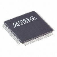
EPM570T100C3N Altera, EPM570T100C3N Datasheet - Page 40

EPM570T100C3N
Manufacturer Part Number
EPM570T100C3N
Description
IC MAX II CPLD 570 LE 100-TQFP
Manufacturer
Altera
Series
MAX® IIr
Specifications of EPM570T100C3N
Programmable Type
In System Programmable
Delay Time Tpd(1) Max
5.4ns
Voltage Supply - Internal
2.5V, 3.3V
Number Of Logic Elements/blocks
570
Number Of Macrocells
440
Number Of I /o
76
Operating Temperature
0°C ~ 85°C
Mounting Type
Surface Mount
Package / Case
100-TQFP, 100-VQFP
Voltage
2.5V, 3.3V
Memory Type
FLASH
Number Of Logic Elements/cells
570
Family Name
MAX II
# Macrocells
440
Frequency (max)
3.01205GHz
Propagation Delay Time
5.4ns
Number Of Logic Blocks/elements
57
# I/os (max)
76
Operating Supply Voltage (typ)
2.5/3.3V
In System Programmable
Yes
Operating Supply Voltage (min)
2.375V
Operating Supply Voltage (max)
3.6V
Operating Temp Range
0C to 85C
Operating Temperature Classification
Commercial
Mounting
Surface Mount
Pin Count
100
Package Type
TQFP
Lead Free Status / RoHS Status
Lead free / RoHS Compliant
Features
-
Lead Free Status / Rohs Status
Compliant
Other names
544-1315
EPM570T100C3N
EPM570T100C3N
Available stocks
Company
Part Number
Manufacturer
Quantity
Price
Part Number:
EPM570T100C3N
Manufacturer:
ALTERA/阿尔特拉
Quantity:
20 000
2–32
Table 2–7. MAX II MultiVolt I/O Support
Referenced Documents
MAX II Device Handbook
Notes to
(1) To drive inputs higher than V
(2) When V
(3) When V
(4) When V
(5) MAX II devices can be 5.0-V tolerant with the use of an external resistor and the internal I/O clamp diode on the EPM1270 and EPM2210
(6) When V
(7) When V
VCCIO (V)
1.5
1.8
2.5
3.3
device, enable the I/O clamp diode to prevent V
devices.
drain setting with internal I/O clamp diode (available only on EPM1270 and EPM2210 devices) and external resistor is required.
Table
CC IO
CC IO
CC IO
CC IO
CC IO
f
2–7:
= 1.8 V, a MAX II device can drive a 1.5-V device with 1.8-V tolerant inputs.
= 3.3 V, a MAX II device can drive a device with 5.0-V TTL inputs but not 5.0-V CMOS inputs. In the case of 5.0-V CMOS, open-
= 2.5 V, a MAX II device can drive a 1.5-V or 1.8-V device with 2.5-V tolerant inputs.
= 3.3 V and a 2.5-V input signal feeds an input pin, the VCCIO supply current will be slightly larger than expected.
= 3.3 V, a MAX II device can drive a 1.5-V, 1.8-V, or 2.5-V device with 3.3-V tolerant inputs.
1.5 V
v
v
—
—
Connect VCCIO pins to either a 1.5-V, 1.8 V, 2.5-V, or 3.3-V power supply, depending
on the output requirements. The output levels are compatible with systems of the
same voltage as the power supply (that is, when VCCIO pins are connected to a 1.5-V
power supply, the output levels are compatible with 1.5-V systems). When VCCIO
pins are connected to a 3.3-V power supply, the output high is 3.3 V and is compatible
with 3.3-V or 5.0-V systems.
For information about output pin source and sink current guidelines, refer to the
428: MAX II CPLD Design
This chapter referenced the following documents:
■
■
■
■
1.8 V
AN 428: MAX II CPLD Design Guidelines
DC and Switching Characteristics
Hot Socketing and Power-On Reset in MAX II Devices
Handbook
Using User Flash Memory in MAX II Devices
v
v
—
—
C CIO
but less than 4.0 V including the overshoot, disable the I/O clamp diode. However, to drive 5.0-V inputs to the
Input Signal
v
2.5 V
v
v
v
(4)
(Note 1)
I
from rising above 4.0 V.
3.3 V
v
v
v
v
Guidelines.
Table 2–7
v
5.0 V
—
—
—
(5)
chapter in the MAX II Device Handbook
summarizes MAX II MultiVolt I/O support.
v
v
v
1.5 V
v
(2)
(3)
(6)
chapter in the MAX II Device Handbook
v
v
1.8 V
v
—
(3)
(6)
chapter in the MAX II Device
Output Signal
v
© October 2008 Altera Corporation
2.5 V
v
—
—
(6)
Chapter 2: MAX II Architecture
Referenced Documents
3.3 V
v
—
—
—
v
5.0 V
—
—
—
(7)
AN


