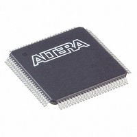
EPM240T100C5N Altera, EPM240T100C5N Datasheet - Page 44

EPM240T100C5N
Manufacturer Part Number
EPM240T100C5N
Description
IC MAX II CPLD 240 LE 100-TQFP
Manufacturer
Altera
Series
MAX® IIr
Specifications of EPM240T100C5N
Programmable Type
In System Programmable
Delay Time Tpd(1) Max
4.7ns
Voltage Supply - Internal
2.5V, 3.3V
Number Of Logic Elements/blocks
240
Number Of Macrocells
192
Number Of I /o
80
Operating Temperature
0°C ~ 85°C
Mounting Type
Surface Mount
Package / Case
100-TQFP, 100-VQFP
Voltage
2.5V, 3.3V
Memory Type
FLASH
Number Of Logic Elements/cells
240
Lead Free Status / RoHS Status
Lead free / RoHS Compliant
Features
-
Other names
544-1964
EPM240T100C5N
EPM240T100C5N
Available stocks
Company
Part Number
Manufacturer
Quantity
Price
Company:
Part Number:
EPM240T100C5N
Manufacturer:
VISHAY
Quantity:
12 000
Company:
Part Number:
EPM240T100C5N
Manufacturer:
ALTERA
Quantity:
8 903
Company:
Part Number:
EPM240T100C5N
Manufacturer:
ALTERA
Quantity:
5 510
Company:
Part Number:
EPM240T100C5N
Manufacturer:
ALTERA
Quantity:
5 000
Part Number:
EPM240T100C5N
Manufacturer:
ALTERA/阿尔特拉
Quantity:
20 000
Part Number:
EPM240T100C5NAH
Manufacturer:
ALTERA/阿尔特拉
Quantity:
20 000
3–2
Table 3–1. MAX II JTAG Instructions (Part 2 of 2)
Table 3–3. 32-Bit MAX II Device IDCODE (Part 1 of 2)
MAX II Device Handbook
CLAMP
USER0
USER1
IEEE 1532
instructions
Notes to
(1) HIGHZ, CLAMP, and EXTEST instructions do not disable weak pull-up resistors or bus hold features.
(2) These instructions are shown in the 1532 BSDL files, which will be posted on the Altera
EPM240
EPM240G
EPM570
EPM570G
EPM1270
EPM1270G
EPM2210
EPM2210G
Device
JTAG Instruction
Table
(1)
3–1:
w
Version
(4 Bits)
0000
0000
0000
0000
Unsupported JTAG instructions should not be issued to the MAX II device as this may
put the device into an unknown state, requiring a power cycle to recover device
operation.
The MAX II device instruction register length is 10 bits and the USERCODE register
length is 32 bits.
device IDCODE information for MAX II devices.
Table 3–2. MAX II Boundary-Scan Register Length
EPM240
EPM570
EPM1270
EPM2210
00 0000 1010
00 0000 1100
00 0000 1110
Instruction Code
Device
0010 0000 1010 0001
0010 0000 1010 0010
0010 0000 1010 0011
0010 0000 1010 0100
(2)
Part Number
Table 3–2
Binary IDCODE (32 Bits)
and
Places the 1-bit bypass register between the TDI and TDO pins,
which allows the boundary scan test data to pass synchronously
through selected devices to adjacent devices during normal device
operation, while holding I/O pins to a state defined by the data in the
boundary-scan register.
This instruction allows you to define the scan chain between TDI
and TDO in the MAX II logic array. This instruction is also used for
custom logic and JTAG interfaces.
This instruction allows you to define the scan chain between TDI
and TDO in the MAX II logic array. This instruction is also used for
custom logic and JTAG interfaces.
IEEE 1532 ISC instructions used when programming a MAX II device
via the JTAG port.
Boundary-Scan Register Length
Table 3–3
000 0110 1110
000 0110 1110
000 0110 1110
000 0110 1110
Identity (11 Bits)
Manufacturer
(1)
show the boundary-scan register length and
240
480
636
816
®
website at
Chapter 3: JTAG and In-System Programmability
IEEE Std. 1149.1 (JTAG) Boundary-Scan Support
Description
www.altera.com
(1 Bit)
© October 2008 Altera Corporation
LSB
1
1
1
1
(2)
when they are available.
0x020A10DD
0x020A20DD
0x020A30DD
0x020A40DD
HEX IDCODE


