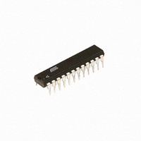
ATF750LVC-15PU Atmel, ATF750LVC-15PU Datasheet - Page 2

ATF750LVC-15PU
Manufacturer Part Number
ATF750LVC-15PU
Description
IC CPLD HS 750 GATE 24-PDIP
Manufacturer
Atmel
Series
ATF750LVCr
Datasheet
1.ATF750LVC-15JC.pdf
(19 pages)
Specifications of ATF750LVC-15PU
Programmable Type
In System Programmable (min 1K program/erase cycles)
Delay Time Tpd(1) Max
15.0ns
Voltage Supply - Internal
3 V ~ 5.5 V
Number Of Macrocells
10
Number Of I /o
10
Operating Temperature
-40°C ~ 85°C
Mounting Type
Through Hole
Package / Case
24-DIP (0.300", 7.62mm)
Voltage
3.3V
Memory Type
EEPROM
Family Name
ATF750LVC
# Macrocells
10
Number Of Usable Gates
500
Frequency (max)
71MHz
Propagation Delay Time
15ns
# I/os (max)
10
Operating Supply Voltage (typ)
3.3V
In System Programmable
No
Operating Supply Voltage (min)
3V
Operating Supply Voltage (max)
3.6V
Operating Temp Range
-40C to 85C
Operating Temperature Classification
Industrial
Mounting
Through Hole
Pin Count
24
Package Type
PDIP
Lead Free Status / RoHS Status
Lead free / RoHS Compliant
Features
-
Number Of Logic Elements/cells
-
Lead Free Status / Rohs Status
Compliant
3. Pin Configurations
2
ATF750LVC
Each of the ATF750LVC’s 22 logic pins can be used as an input. Ten of these can be used as
inputs, outputs or bi-directional I/O pins. Each flip-flop is individually configurable as either
D- or T-type. Each flip-flop output is fed back into the array independently. This allows burying
of all the sum terms and flip-flops.
There are 171 total product terms available. There are two sum terms per output, providing
added flexibility. A variable format is used to assign between four to eight product terms per
sum term. Much more logic can be replaced by this device than by any other 24-pin PLD. With
20 sum terms and flip-flops, complex state machines are easily implemented with logic to
spare.
Product terms provide individual clocks and asynchronous resets for each flip-flop. Each flip-
flop may also be individually configured to have direct input pin controlled clocking. Each out-
put has its own enable product term. One product term provides a common synchronous
preset for all flip-flops. Register preload functions are provided to simplify testing. All registers
automatically reset upon power-up.
Pin Name
CLK
IN
I/O
GND
VCC
3.1
Note:
GND
IN
IN
IN
IN
IN
IN
PLCC
1. For PLCC, pins 1, 8, 15, and 22 can
(1)
be left unconnected. For superior
performance, connect VCC to pin 1
and GND to pins 8, 15, and 22.
5
6
7
8
9
10
11
Function
Clock
Logic Inputs
Bi-directional Buffers
Ground
3V to 5.5V Supply
25
24
23
22
21
20
19
I/O
I/O
I/O
GND
I/O
I/O
I/O
(1)
3.2
DIP/SOIC/TSSOP
CLK/IN
GND
IN
IN
IN
IN
IN
IN
IN
IN
IN
IN
1
2
3
4
5
6
7
8
9
10
11
12
24
23
22
21
20
19
18
17
16
15
14
13
VCC
I/O
I/O
I/O
I/O
I/O
I/O
I/O
I/O
I/O
I/O
IN
1447F–PLD–11/08


