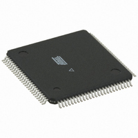
ATF1504BE-7AU100 Atmel, ATF1504BE-7AU100 Datasheet - Page 10

ATF1504BE-7AU100
Manufacturer Part Number
ATF1504BE-7AU100
Description
IC CPLD 64MC 1.8V 100-TQFP
Manufacturer
Atmel
Series
ATF1504BEr
Datasheet
1.ATF1504BE-7AU44.pdf
(30 pages)
Specifications of ATF1504BE-7AU100
Programmable Type
In System Programmable (min 10K program/erase cycles)
Delay Time Tpd(1) Max
7.5ns
Voltage Supply - Internal
1.7 V ~ 1.9 V
Number Of Macrocells
64
Number Of I /o
80
Operating Temperature
-40°C ~ 85°C
Mounting Type
Surface Mount
Package / Case
100-TQFP, 100-VQFP
Features
CMOS/TTL Compatible
Voltage
1.8V
Memory Type
CMOS
For Use With
ATF15XX-DK3 - KIT DEV FOR ATF15XX CPLD'S
Lead Free Status / RoHS Status
Lead free / RoHS Compliant
Number Of Logic Elements/cells
-
Available stocks
Company
Part Number
Manufacturer
Quantity
Price
Company:
Part Number:
ATF1504BE-7AU100
Manufacturer:
TI
Quantity:
1 450
Part Number:
ATF1504BE-7AU100
Manufacturer:
ATMEL/爱特梅尔
Quantity:
20 000
3. Power Management
4. Security Feature
5. Programming Methods
10
ATF1504BE
Unlike conventional CPLDs with sense amplifiers, the ATF1504BE is designed using low-power
full CMOS design techniques. This enables the ATF1504BE to achieve extremely low power
consumption over the full operating frequency spectrum.
The ATF1504BE also has an optional power-down mode. In this mode, current drops to below
100 µA. When the power-down option is selected, either PD1 or PD2 pins (or both) can be used
to power down the part. When enabled, the device goes into power-down when either PD1 or
PD2 is high. In the power-down mode, all internal logic signals are latched and held, as are any
enabled outputs.
All pin transitions are ignored until the PD pin is brought low. When the power-down feature is
enabled, the PD1 or PD2 pin cannot be used as a logic input or output. However, the pin’s mac-
rocell may still be used to generate buried foldback and cascade logic signals.
All power-down AC characteristic parameters are computed from external input or I/O pins.
A fuse is provided to prevent unauthorized copying of the ATF1504BE fuse patterns. Once
enabled, fuse reading or verification is inhibited. However, the 16-bit User Electronic Signature
remains accessible. To reset this feature, the entire memory array in the device must be erased.
The ATF1504BE devices are In-System Programmable (ISP) or In-System Configurable (ISC)
devices utilizing the 4-pin JTAG protocol. This capability eliminates package handling normally
required for programming and facilitates rapid design iterations and field changes.
When using the ISP hardware or software to program the ATF1504BE devices, four I/O pins
must be reserved for the JTAG interface. However, the logic features that the macrocells have
associated with these I/O pins are still available to the design for buried logic functions.
To facilitate ISP programming by the Automated Test Equipment (ATE) vendors, Serial Vector
Format (SVF) files can be created by Atmel-provided software utilities. ATF1504BE devices can
also be programmed using standard third-party programmers. With a third-party programmer,
the JTAG ISP port can be disabled, thereby allowing four additional I/O pins to be used for logic.
The AT1504BE device supports several configuration modes which gives designers several
unique options for programming.
The different modes of programming are:
• ISC – In-System Configuration
• OTF – On-the-Fly Reconfiguration
• DRA – Direct Reconfiguration Access
3637B–PLD–1/08


