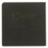
XC9572-10PCG84C Xilinx Inc, XC9572-10PCG84C Datasheet - Page 14

XC9572-10PCG84C
Manufacturer Part Number
XC9572-10PCG84C
Description
IC CPLD 72MCRCELL 10NS 84PLCC
Manufacturer
Xilinx Inc
Series
XC9500r
Specifications of XC9572-10PCG84C
Programmable Type
In System Programmable (min 10K program/erase cycles)
Delay Time Tpd(1) Max
10.0ns
Voltage Supply - Internal
4.75 V ~ 5.25 V
Number Of Logic Elements/blocks
4
Number Of Macrocells
72
Number Of Gates
1600
Number Of I /o
69
Operating Temperature
0°C ~ 70°C
Mounting Type
Surface Mount
Package / Case
84-PLCC
Voltage
5V
Memory Type
FLASH
Lead Free Status / RoHS Status
Lead free / RoHS Compliant
Features
-
Number Of Logic Elements/cells
-
Other names
122-1440
Available stocks
Company
Part Number
Manufacturer
Quantity
Price
Company:
Part Number:
XC9572-10PCG84C
Manufacturer:
BROADCOM
Quantity:
201
Company:
Part Number:
XC9572-10PCG84C
Manufacturer:
XILINX
Quantity:
186
Part Number:
XC9572-10PCG84C
Manufacturer:
XILINX/赛灵思
Quantity:
20 000
XC9500 In-System Programmable CPLD Family
Low Power Mode
All XC9500 devices offer a low-power mode for individual
macrocells or across all macrocells. This feature allows the
device power to be significantly reduced.
Each individual macrocell may be programmed in
low-power mode by the user. Performance-critical parts of
the application can remain in standard power mode, while
other parts of the application may be programmed for
low-power operation to reduce the overall power dissipa-
tion. Macrocells programmed for low-power mode incur
additional delay (T
well as register setup time. Product term clock to output and
product term output enable delays are unaffected by the
macrocell power-setting.
Timing Model
The uniformity of the XC9500 architecture allows a simpli-
fied timing model for the entire device. The basic timing
14
Figure 13: In-System Programming Operation (a) Solder Device to PCB and (b) Program Using Download Cable
LP
) in pin-to-pin combinatorial delay as
(a)
www.xilinx.com
model, shown in
that use the direct product terms only, with standard power
setting, and standard slew rate setting.
each of the key timing parameters is affected by the product
term allocator (if needed), low-power setting, and slew-lim-
ited setting.
The product term allocation time depends on the logic span
of the macrocell function, which is defined as one less than
the maximum number of allocators in the product term path.
If only direct product terms are used, then the logic span is
0. The example in
terms are available with a span of 1. In the case of
the 18 product term function has a span of 2.
Detailed timing information may be derived from the full tim-
ing model shown in
for each parameter are given in the individual device data
sheets.
Figure
Figure
Figure 6
(b)
14, is valid for macrocell functions
15. The values and explanations
shows that up to 15 product
DS063 (v5.5) June 25, 2007
Product Specification
X5902
Table 4
shows how
Figure
7,
R


