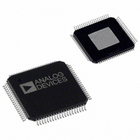
AD9786BSV Analog Devices Inc, AD9786BSV Datasheet - Page 30

AD9786BSV
Manufacturer Part Number
AD9786BSV
Description
IC DAC 16BIT INTERPOL/SP 80-TQFP
Manufacturer
Analog Devices Inc
Series
TxDAC+®r
Datasheet
1.AD9786BSVZRL.pdf
(56 pages)
Specifications of AD9786BSV
Number Of Bits
16
Data Interface
Parallel
Number Of Converters
1
Voltage Supply Source
Single Supply
Power Dissipation (max)
1.25W
Operating Temperature
-40°C ~ 85°C
Mounting Type
Surface Mount
Package / Case
80-TQFP Exposed Pad, 80-eTQFP, 80-HTQFP, 80-VQFP
For Use With
AD9786-EB - BOARD EVALUATION FOR AD9786
Lead Free Status / RoHS Status
Contains lead / RoHS non-compliant
Settling Time
-
Available stocks
Company
Part Number
Manufacturer
Quantity
Price
Company:
Part Number:
AD9786BSV
Manufacturer:
ADI
Quantity:
193
Part Number:
AD9786BSV
Manufacturer:
ADI/亚德诺
Quantity:
20 000
Company:
Part Number:
AD9786BSVZ
Manufacturer:
ADI
Quantity:
200
Company:
Part Number:
AD9786BSVZ
Manufacturer:
Analog Devices Inc
Quantity:
10 000
Part Number:
AD9786BSVZ
Manufacturer:
ADI/亚德诺
Quantity:
20 000
Company:
Part Number:
AD9786BSVZRL
Manufacturer:
Analog Devices Inc
Quantity:
10 000
AD9786
Note that the data in Figure 44 to Figure 53 was taken with the
DATAADJ default of 0000. Changing the DATAADJ values allows
the user to select the specific edge of DACCLK upon which the
input data is latched. This can be done in master mode, but it
is most useful in slave mode. For more information on using
DATAADJ and MODADJ to synchronize multiple AD9786s,
see Analog Devices Application Note 747. Table 27 lists the values
available for 8× interpolation, which, in turn, provides a choice of
16 edges to sync data. With 4× interpolation, there is
a choice of eight edges, and the relevant values from Table 27
are 0000, 0010, 0100, 0110, 1000, 1010, 1100, and 1110. These
options allow latching edge placement from +3 cycles to −4 cycles.
In 2× interpolation, four edges are available, and the relevant
values from Table 27 are 0000, 0100, 1000, and 1100. The
choices for DATAADJ are diminished to +1 cycle to –2 cycles.
Figure 54, Figure 55, and Figure 56 show the alignment for the
latching edge of DACCLK with 4× interpolation and different
settings for DATAADJ. In Figure 54, the AD9786 is in
DATACLK master mode. DATAADJ is set to 0000, with
DCLKPOL set to 0 so that the latching edge of DACCLK is
immediately before the rising edge of DATACLK. The data
transitions shown in Figure 54 are synchronous with the
DACCLK, so that DACCLK and input data are constant with
respect to each other.
The only visible change when DATAADJ is altered is that
DATACLK moves, indicating the latching edge has moved as
well. Note that in DATACLK master mode, when DATAADJ is
altered, the latching edge with respect to DATACLK remains
the same.
DATA TRANSITION
Figure 54. DATAADJ = 0000
DACCLK
LATCHING EDGE
RISING EDGE OF DATACLK
CONCURRENT WITH
LATCHING EDGE OF DACCLK
Rev. B | Page 30 of 56
Figure 55 shows the same conditions, but with DATAADJ set to
1111. This moves DATACLK to the left in the plot, indicating that
it occurs one DACCLK cycle before it did in Figure 54; therefore,
the latching edge of DACCLK also occurs one cycle earlier.
Figure 56 shows the same conditions, with DATAADJ set
to 0001; therefore, DATACLK moves to the right in the plot.
This indicates that it occurs one DACCLK cycle after it did in
Figure 54; therefore, the latching edge of DACCLK also occurs
one cycle later.
DATA TRANSITION
LATCHING EDGE
DATA TRANSITION
DACCLK
Figure 55. DATAADJ = 1111
Figure 56. DATAADJ = 0001
RISING EDGE OF DATACLK
CONCURRENT WITH
LATCHING EDGE OF DACCLK
LATCHING EDGE
RISING EDGE OF DATACLK
CONCURRENT WITH
LATCHING EDGE OF DACCLK
DACCLK


