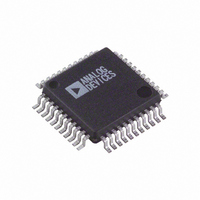
AD7835AS Analog Devices Inc, AD7835AS Datasheet - Page 6

AD7835AS
Manufacturer Part Number
AD7835AS
Description
IC DAC 14BIT QUAD PARA 44-MQFP
Manufacturer
Analog Devices Inc
Datasheet
1.AD7835ASZ.pdf
(28 pages)
Specifications of AD7835AS
Rohs Status
RoHS non-compliant
Settling Time
10µs
Number Of Bits
14
Data Interface
Parallel
Number Of Converters
4
Voltage Supply Source
Analog and Digital, Dual ±
Power Dissipation (max)
465mW
Operating Temperature
-40°C ~ 85°C
Mounting Type
Surface Mount
Package / Case
44-MQFP, 44-PQFP
Available stocks
Company
Part Number
Manufacturer
Quantity
Price
Company:
Part Number:
AD7835AS
Manufacturer:
AD
Quantity:
13 888
Company:
Part Number:
AD7835ASZ
Manufacturer:
OKI
Quantity:
490
Company:
Part Number:
AD7835ASZ
Manufacturer:
ADI
Quantity:
850
Company:
Part Number:
AD7835ASZ
Manufacturer:
Analog Devices Inc
Quantity:
10 000
Part Number:
AD7835ASZ
Manufacturer:
ADI/亚德诺
Quantity:
20 000
Company:
Part Number:
AD7835ASZ-REEL
Manufacturer:
Analog Devices Inc
Quantity:
10 000
AD7834/AD7835
TIMING SPECIFICATIONS
V
Table 4.
Parameter
AD7834-SPECIFIC
AD7835-SPECIFIC
GENERAL
1
2
(SIMULTANEOUS
All input signals are specified with t
Rise and fall times should be no longer than 50 ns.
(PER-CHANNEL
CC
t
t
t
t
t
t
t
t
t
t
t
t
t
t
t
t
t
t
t
t
t
1
2
3
4
5
6
7
8
9
21
11
12
13
14
15
16
17
18
19
20
10
2
2
2
= 5 V ± 5%; V
UPDATE)
UPDATE)
FSYNC
SCLK
LDAC
LDAC
DIN
MSB
DD
Figure 3. AD7834 Timing Diagram
= 11.4 V to 15.75 V; V
CLK
1ST
t
4
D23
t
8
t
7
2ND
CLK
t
6
D22
r
Limit at T
100
50
30
30
40
30
10
0
40
20
15
15
0
0
40
40
10
0
0
0
40
= t
f
= 5 ns (10% to 90% of 5 V) and time from a voltage level of 1.6 V.
t
2
t
MIN
1
t
3
, T
SS
D1
24TH
CLK
= −11.4 V to −15.75 V; AGND = DGND = 0 V
MAX
D0
t
5
LSB
t
t
9
t
21
10
Rev. D | Page 6 of 28
Unit
ns min
ns min
ns min
ns min
ns min
ns min
ns min
ns min
ns min
ns min
ns min
ns min
ns min
ns min
ns min
ns min
ns min
ns min
ns min
ns min
ns min
(SIMULTANEOUS
(PER-CHANNEL
DB0 TO DB13
UPDATE)
A0 A1 A2
UPDATE)
Description
SCLK low
FSYNC, PAEN setup time
FSYNC, PAEN hold time
LDAC to FSYNC setup time
LDAC to FSYNC hold time
Delay between write operations
A0, A1, A2, BYSHF to CS setup time
A0, A1, A2, BYSHF to CS hold time
CS to WR setup time
CS to WR hold time
WR pulse width
LDAC to CS setup time
CS to LDAC setup time
LDAC to CS hold time
LDAC, CLR pulse width
SCLK cycle time
SCLK high time
Data setup time
Data hold time
Data setup time
Data hold time
BYSHF
LDAC
LDAC
WR
CS
Figure 4. AD7835 Timing Diagram
t
1
13
.
t
t
18
11
t
15
t
16
t
17
t
20
t
t
14
19
t
12
t
10


