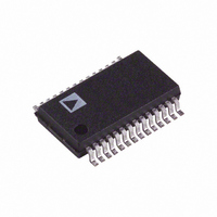
AD5554BRS Analog Devices Inc, AD5554BRS Datasheet - Page 10

AD5554BRS
Manufacturer Part Number
AD5554BRS
Description
IC DAC 14BIT QUAD SERIAL 28-SSOP
Manufacturer
Analog Devices Inc
Datasheet
1.AD5554BRSZ.pdf
(16 pages)
Specifications of AD5554BRS
Rohs Status
RoHS non-compliant
Settling Time
2µs
Number Of Bits
14
Data Interface
Serial
Number Of Converters
4
Voltage Supply Source
Dual ±
Power Dissipation (max)
1.25mW
Operating Temperature
-40°C ~ 85°C
Mounting Type
Surface Mount
Package / Case
28-SSOP
Available stocks
Company
Part Number
Manufacturer
Quantity
Price
Part Number:
AD5554BRSZ
Manufacturer:
ADI/亚德诺
Quantity:
20 000
AD5544/AD5554
THEORY OF OPERATION
The AD5544 and the AD5554 contain four 16-bit and 14-bit,
current output DACs, respectively. Each DAC has its own inde-
pendent multiplying reference input. Both the AD5544 and the
AD5554 use a 3-wire, SPI-compatible serial data interface, with
a configurable asynchronous RS pin for half-scale (MSB = 1) or
zero-scale (MSB = 0) preset. In addition, an LDAC strobe enables
four-channel, simultaneous updates for hardware synchronized
output voltage changes.
DIGITAL-TO-ANALOG CONVERTER (DAC)
Each part contains four current-steering R-2R ladder DACs.
Figure 18 shows a typical equivalent DAC. Each DAC contains
a matching feedback resistor for use with an external I-to-V
converter amplifier. The R
external amplifier. The I
input of the external amplifier. The A
connected to the load point, requiring full 16-bit accuracy. These
DACs are designed to operate with both negative and positive
reference voltage. The V
to drive the DAC switches on and off. Note that a matching switch
is used in series with the internal 5 kΩ feedback resistor. If users
attempt to measure the value of R
to achieve continuity. An additional V
the substrate during high temperature applications, minimizing
zero-scale leakage currents that double every 10°C. The DAC
output voltage is determined by V
the following equations:
Note that the output polarity is opposite the V
reference voltages.
V
REF
X
V
V
OUT
OUT
DIGITAL INTERFACE CONNECTIONS OMITTED FOR CLARITY.
SWITCHES S1 AND S2 ARE CLOSED, V
V
2R
SS
=
=
−
−
DGND
Figure 18. Typical Equivalent DAC Channel
V
V
R
REF
REF
2R
×
×
FROM OTHER DACS A
16384
65536
D
D
OUT
DD
FB
power pin is only used by the logic
x terminal connects to the inverting
x pin connects to the output of the
R
(
(
for
for
2R
FB
, power must be applied to V
the
REF
the
GND
R
DD
SS
and the digital data (D) in
AD
AD
GND
x pin should be Kelvin-
bias pin is used to guard
MUST BE POWERED.
R
5544
5554
S2
5kΩ
REF
)
)
polarity for dc
S1
V
R
A
I
A
OUT
DD
FB
GND
GND
X
X
X
F
Rev. D | Page 10 of 16
DD
(1)
(2)
These DACs are also designed to accommodate ac reference input
signals. Both the AD5544 and the AD5554 accommodate input
reference voltages in the range of −15 V to +15 V. The reference
voltage inputs exhibit a constant nominal input resistance of 5 kΩ ±
30%. On the other hand, the I
DAC outputs are code dependent and produce various output
resistances and capacitances. The choice of external amplifier
should take into account the variation in impedance generated by
the AD5544/AD5554 on the inverting input node of the amplifier.
The feedback resistance, in parallel with the DAC ladder resistance,
dominates output voltage noise. For multiplying mode applications,
an external feedback compensation capacitor, C
to provide a critically damped output response for step changes in
reference input voltages. Figure 19 shows the gain vs. frequency
performance at various attenuation settings using a 23 pF external
feedback capacitor connected across the I
for the AD5544 and the AD5554, respectively. To maintain good
analog performance, power supply bypassing of 0.01 μF, in parallel
with 1 μF, is recommended. Under these conditions, a clean power
supply with low ripple voltage capability should be used. Switching
power supplies is usually not suitable for this application, due to
the higher ripple voltage and PSS frequency-dependent charac-
teristics. It is best to derive the supply of the AD5544/AD5554
from system analog supply voltages. Do not use the digital
supply (see Figure 20).
Figure 19. AD5554 Reference Multiplying Bandwidth vs. Code
–2
–4
–6
–8
100k
2
0
1M
FREQUENCY (Hz)
OUT
A, I
OUT
B, I
10M
OUT
OUT
x and R
C, and I
FB
, may be needed
FB
x terminals
OUT
100M
D


