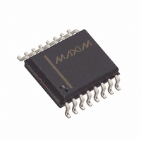
MAX532BCWE Maxim Integrated Products, MAX532BCWE Datasheet - Page 6

MAX532BCWE
Manufacturer Part Number
MAX532BCWE
Description
IC MDAC DUAL V-OUT 12BIT 16-SOIC
Manufacturer
Maxim Integrated Products
Datasheet
1.MAX532ACPE.pdf
(16 pages)
Specifications of MAX532BCWE
Settling Time
2.5µs
Number Of Bits
12
Data Interface
Serial
Number Of Converters
2
Voltage Supply Source
Dual ±
Power Dissipation (max)
762mW
Operating Temperature
0°C ~ 70°C
Mounting Type
Surface Mount
Package / Case
16-SOIC (0.300", 7.5mm Width)
Lead Free Status / RoHS Status
Contains lead / RoHS non-compliant
Available stocks
Company
Part Number
Manufacturer
Quantity
Price
Company:
Part Number:
MAX532BCWE
Manufacturer:
MAXIM
Quantity:
36
Part Number:
MAX532BCWE
Manufacturer:
MAXIM/美信
Quantity:
20 000
Company:
Part Number:
MAX532BCWE+
Manufacturer:
Maxim
Quantity:
42
Company:
Part Number:
MAX532BCWE+
Manufacturer:
IDT
Quantity:
107
Part Number:
MAX532BCWE+T
Manufacturer:
MAXIM/美信
Quantity:
20 000
Dual, Serial-Input,
Voltage-Output, 12-Bit MDAC
(V
6
______________________________________________________________Pin Description
____________________________Typical Operating Characteristics (continued)
DD
AGNDA
_______________________________________________________________________________________
= 15V, V
PIN
10
11
12
13
14
15
16
1
2
3
4
5
6
7
8
9
A = V
TIMEBASE = 2 s/div
V
REFA
SS
OUTA
= ±100mV SQUARE WAVE
SMALL-SIGNAL PULSE RESPONSE
= -15V, R
, 50mV/div
AGNDA
AGNDB
VOUTA
VOUTB
VREFA
VREFB
NAME
DGND
DOUT
RFBA
RFBB
SCLK
LDAC
V
V
DIN
CS
DD
L
SS
= 2kΩ, C
L
Feedback Resistor for DACA
Reference Input for DACA
Voltage Output for DACA
Analog Ground for DACA
Analog Ground for DACB
Voltage Output for DACB
Reference Input for DACB
Feedback Resistor for DACB
Negative Supply Voltage
Digital Ground
Serial Clock Input
Serial Data Output. Open-drain N-channel MOSFET output: requires external pull-up resis-
tor. Data on DOUT changes on the falling edge of SCLK. Serial output data is delayed 24
clock cycles from DIN.
Serial Data Input. CMOS- and TTL-compatible input. Data is clocked into DIN on the rising
edge of SCLK. CS must be low for data to be clocked in.
Chip-Select Input, active low. Data is shifted in and out when CS is low. DAC latches are
updated when CS is high and LDAC is low.
Asynchronous Load DAC Input, active low. DAC latches are updated when CS is high and
LDAC is low.
Positive Supply Voltage
= 100pF, unless otherwise noted.)
A
AGNDA
FUNCTION
A = VOUTA, 5V/div
TIMEBASE = 2 s/div
VREFA = ±10V SQUARE WAVE
LARGE-SIGNAL PULSE RESPONSE
A


