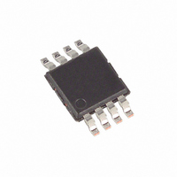
MAX5721EUA+ Maxim Integrated Products, MAX5721EUA+ Datasheet - Page 11

MAX5721EUA+
Manufacturer Part Number
MAX5721EUA+
Description
IC DAC 10BIT DUAL LP SER 8-UMAX
Manufacturer
Maxim Integrated Products
Datasheet
1.MAX5721AUA.pdf
(14 pages)
Specifications of MAX5721EUA+
Settling Time
4µs
Number Of Bits
10
Data Interface
Serial
Number Of Converters
2
Voltage Supply Source
Single Supply
Operating Temperature
-40°C ~ 85°C
Mounting Type
Surface Mount
Package / Case
8-MSOP, Micro8™, 8-uMAX, 8-uSOP,
Number Of Dac Outputs
2
Resolution
10 bit
Interface Type
Serial (SPI)
Supply Voltage (max)
5.5 V
Supply Voltage (min)
2.7 V
Maximum Operating Temperature
+ 125 C
Mounting Style
SMD/SMT
Maximum Power Dissipation
362 mW
Minimum Operating Temperature
- 40 C
Supply Current
135 uA
Voltage Reference
External
Lead Free Status / RoHS Status
Lead free / RoHS Compliant
Power Dissipation (max)
-
Lead Free Status / Rohs Status
Lead free / RoHS Compliant
Table 2. Serial-Interface Programming Commands
X = Don’t Care
The typical application circuit (Figure 3) shows the
MAX5721 configured for a unipolar output, where the
output voltages and the reference inputs have the
same polarity. Table 3 lists the unipolar output codes.
The MAX5721 can be configured for bipolar operation
using a dual supply op amp (Figure 4). The transfer
function for bipolar operation is:
Figure 3. Typical Operating Circuit, Unipolar Output
C3
0
0
0
0
1
1
1
1
1
IN
MAX6050
GND
CONTROL
C2
0
0
1
1
0
0
1
1
1
OUT
C1
0
0
0
0
0
0
0
0
1
Applications Information
V
OUT
______________________________________________________________________________________
10-Bit, Low-Power, Dual, Voltage-Output
C0
0
1
0
1
0
1
0
1
0
DAC_
V
REF
D9–D0
REF
DATA BITS
X
X
X
X
X
X
X
X
X
GND
1024
2D
S1–S0
X
X
X
X
X
X
X
X
X
+2.7V to +5.5V
Unipolar Output
Bipolar Output
V
MAX5721
1
DD
DAC
A-B
A-B
A-B
A
B
A
B
A
B
Input register transparent, data shifted directly to DAC register, OUTA updated
Input register transparent, data shifted directly to DAC register, OUTB updated
Data shifted to input register, OUTA unchanged
Data shifted to input register, OUTB unchanged
Shift data from input register to DAC register, OUTA updated
Shift data from input register to DAC register, OUTB updated
Input registers transparent, data shifted directly to DAC registers, OUTA and
OUTB updated
Data shifted to input registers, OUTA and OUTB unchanged
Shift data from input registers to DAC registers, OUTA and OUTB updated
OUT_
DAC with Serial Interface
where DB is the decimal value of the DACs binary input
code. Table 4 shows digital codes (offset binary) and
corresponding output voltages for the circuit in Figure 4.
Careful PC board layout is important for optimal system
performance. To reduce noise injection and digital feed-
through, keep analog and digital signals separate.
Ensure that that the return path from GND to the supply
ground is short and low impedance. Use a ground
plane. Bypass V
close as possible to V
Figure 4. Bipolar Output Circuit
Power Supply and Layout Considerations
DAC_
REF
GND
FUNCTION
DD
R1
+2.7V to +5.5V
to GND with a 0.1µF capacitor as
MAX5721
DD
V
.
DD
OUT_
R1 = R2
V+
V-
R2
V
OUT
11


