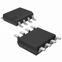
MAX5541CSA Maxim Integrated Products, MAX5541CSA Datasheet

MAX5541CSA
Specifications of MAX5541CSA
Available stocks
Related parts for MAX5541CSA
MAX5541CSA Summary of contents
Page 1
... Unbuffered Voltage Output Directly Drives 60kΩ Loads o SPI/QSPI/MICROWIRE-Compatible Serial Interface o Power-On Reset Circuit Clears DAC Output to 0V (unipolar mode) o Schmitt Trigger Inputs for Direct Optocoupler Interface o Choose MAX541 as a 1LSB (max) INL Upgrade to the MAX5541 PART MAX5541CSA MAX5541ESA REF DGND 7 CS DIN ...
Page 2
... Reference -3dB Bandwidth BW Reference Feedthrough Signal-to-Noise Ratio SNR Reference Input Capacitance _______________________________________________________________________________________ Operating Temperature Ranges MAX5541CSA .....................................................0°C to +70°C +0.3V) MAX5541ESA ..................................................-40°C to +85°C DD Junction Temperature ......................................................+150°C Storage Temperature Range .............................-65°C to +150°C DD Lead Temperature (soldering, 10s) ................................ +300° unless otherwise noted. Typical values are at T ...
Page 3
ELECTRICAL CHARACTERISTICS (continued +5V ±5 +2.5V REF AGND PARAMETER SYMBOL STATIC PERFORMANCE—REFERENCE SECTION STATIC PERFORMANCE—DIGITAL INPUTS Input High Voltage Input Low Voltage Input Current Input Capacitance Hysteresis Voltage POWER SUPPLY Positive Supply Range V ...
Page 4
Low-Cost, +5V, Serial-Input, Voltage-Output, 16-Bit DAC (V = +5V +2.5V +25°C, unless otherwise noted.) DD REF A SUPPLY CURRENT vs. TEMPERATURE 0.50 0.45 0.40 0.35 0.30 0.25 0.20 -40 - 100 ...
Page 5
V = +2.5V +25°C, unless otherwise noted.) DD REF A FULL-SCALE STEP RESPONSE (f SCLK 1µs/div = ∞ 13pF MAJOR-CARRY OUTPUT GLITCH 2µs/div PIN NAME 1 OUT 2 AGND 3 ...
Page 6
Low-Cost, +5V, Serial-Input, Voltage-Output, 16-Bit DAC Detailed Description The MAX5541 voltage-output, 16-bit digital-to-analog converter (DAC) offers 16-bit monotonicity with less than 1LSB differential linearity error. Serial-data transfer minimizes the number of package pins required. The MAX5541 is composed of two ...
Page 7
Applications Information Reference and Analog Ground Inputs The MAX5541 operates with external voltage references from 2V to 3V, and maintains 16-bit performance with proper reference selection and application. Ideally, the reference’s temperature coefficient should be less than 0.4ppm/°C to maintain ...
Page 8
Low-Cost, +5V, Serial-Input, Voltage-Output, 16-Bit DAC The external buffer amplifier’s gain-bandwidth product is important because it increases the settling time by adding another time constant to the output response. The effective time constant of two cascaded systems, each with a ...
Page 9
... Maxim cannot assume responsibility for use of any circuitry other than circuitry entirely embodied in a Maxim product. No circuit patent licenses are implied. Maxim reserves the right to change the circuitry and specifications without notice at any time. 9 _____________________Maxim Integrated Products, 120 San Gabriel Drive, Sunnyvale, CA 94086 408-737-7600 © 2002 Maxim Integrated Products ...


