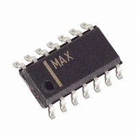
MAX512CSD+T Maxim Integrated Products, MAX512CSD+T Datasheet - Page 9

MAX512CSD+T
Manufacturer Part Number
MAX512CSD+T
Description
IC DAC 8BIT TRIPLE SERIAL 14SOIC
Manufacturer
Maxim Integrated Products
Datasheet
1.MAX512CPD.pdf
(16 pages)
Specifications of MAX512CSD+T
Settling Time
70µs
Number Of Bits
8
Data Interface
Serial
Number Of Converters
3
Voltage Supply Source
Dual ±
Operating Temperature
0°C ~ 70°C
Mounting Type
Surface Mount
Package / Case
14-SOIC (3.9mm Width), 14-SOL
Lead Free Status / RoHS Status
Lead free / RoHS Compliant
Power Dissipation (max)
-
The MAX512/MAX513 contain three 8-bit, voltage-out-
put, digital-to-analog converters (DACs). The DACs are
“inverted” R-2R ladder networks using complementary
switches that convert 8-bit digital inputs into equivalent
analog output voltages in proportion to the applied ref-
erence voltages.
The MAX512/MAX513 have two reference inputs: one is
shared by DAC A and DAC B and the other is used by
DAC C. These inputs allow different full-scale output
voltages and different output voltage polarities for the
DAC pair A/B and DAC C.
The MAX512/MAX513 include output buffer amplifiers
for DACs A and B and input logic for simple micro-
processor (µP) and CMOS interfaces.
The MAX512/MAX513 operate in either single-supply or
dual-supply mode, as determined by V
in approximately -0.5V of GND, single-supply mode is
assumed. If V
supply mode.
The voltage at REF_ sets the full-scale output of the
DACs. The input impedance of the REF_ inputs is code
dependent. The lowest value, approximately 12kΩ for
REFC (8kΩ for REFAB), occurs when the input code is
01010101 (55hex). The maximum value of infinity
occurs when the input code is zero.
In shutdown mode, the selected DAC output is set to
zero while the value stored in the DAC register remains
unchanged. This removes the load from the reference
input to save power. Bringing the MAX512/MAX513 out
of shutdown mode restores the DAC output voltage.
Because the input resistance at REF_ is code depen-
dent, the DAC’s reference sources should have an out-
put impedance of no more than 5Ω. The input capaci-
tance at the REF_ pins is also code dependent and
typically does not exceed 25pF.
The reference voltage on REFAB can range anywhere
between the supply rails. In dual-supply mode, a posi-
tive reference input voltage on REFAB should be less
than (V
fiers. The reference voltage includes the negative sup-
ply rail. See the Output Buffer Amplifier section for more
information. The REFC input accepts positive voltages
up to V
The absolute difference between any reference voltage
and GND should not exceed 6V.
_______________Detailed Description
DD
DD
Low-Cost, Triple, 8-Bit Voltage-Output DACs
and should not be forced below ground.
- 1.5V) to avoid saturating the buffer ampli-
Reference Inputs and DAC Output Range
SS
is below -1.5V, the devices are in dual-
_______________________________________________________________________________________
Analog Section
SS
. If V
SS
is with-
DAC A and DAC B voltage outputs are internally
buffered. The buffer amplifiers have a rail-to-rail
(V
In single-supply mode, the DAC outputs A and B are
internally divided by two and the buffer is set to a gain
of two, eliminating the need for a buffer input voltage
range to the positive supply rail.
In dual-supply mode, the DAC outputs are not attenuat-
ed and the buffer is set to unity gain.
Although only necessary for negative output voltages,
the dual-supply mode may be used even if the desired
DAC output voltage is positive. Possible errors associ-
ated with the divide-by-two attenuator and gain-of-two
buffers in single-supply mode are eliminated in dual-
supply mode. In this case, do not use reference volt-
ages higher than (V
DAC A’s output amplifier can source and sink up to 5mA
of current (0.5mA for DAC B buffer). See the Total
Unadjusted Error vs. Digital Code graph in the Typical
Operating Characteristics for dual and single supplies.
The amplifier is unity-gain stable with a capacitive load of
0.05µF (0.01µF for DAC B buffer) or greater. The slew
rate is limited by the load capacitor and is typically
0.1V/µs with a 0.1µF load (0.01µF for DAC B buffer).
The output of DAC C is unbuffered and has a typical out-
put impedance of 24kΩ. It can be used to drive a high-
impedance load, such as an op amp or comparator, and
has 35µs typical settling time to 1/2LSB with a single 3V
supply. Use DAC C if a quick dynamic response is
required.
Figure 1. DAC Simplified Circuit Diagram
SS
GND
REF
to V
with Serial Interface
DD
2R
Output Buffer Amplifiers (DAC A / DAC B)
) output voltage range.
2R
R
DD
SHOWN FOR ALL 1s ON DAC; DAC C IS NOT BUFFERED
- 1.5V).
2R
R
Unbuffered Output (DAC C)
2R
R
2R
OUT
9


