LM4850LDX National Semiconductor, LM4850LDX Datasheet
LM4850LDX
Specifications of LM4850LDX


Related parts for LM4850LDX

LM4850LDX Summary of contents
Page 1
... LM4850LD, LM4850MM, and LM4850MT. Typical Application FIGURE 1. Typical Audio Amplifier Application Circuit Boomer ® registered trademark of National Semiconductor Corporation. © 2002 National Semiconductor Corporation Key Specifications n Output Power at 1% THD+N, 1kHz: LM4850LD 3Ω BTL n LM4850LD 4Ω ...
Page 2
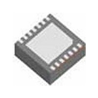
Connection Diagrams www.national.com 20001051 Top View 10 Lead MSOP Order Number LM4850MM See NS Package Number MUB10A Top View 14 Lead TSSOP Order Number LM4850MT See NS Package Number MTC14 Top View 14 Lead LLP Order Number LM4850LD See NS ...
Page 3
... Absolute Maximum Ratings If Military/Aerospace specified devices are required, please contact the National Semiconductor Sales Office/ Distributors for availability and specifications. Supply Voltage Storage Temperature ESD Susceptibility (Note 5) ESD Machine model (Note 8) Junction Temperature ( Solder Information (Note 2) Small Outline Package Vapor Phase (60 sec.) Infrared (15 sec ...
Page 4
Electrical Characteristics The following specifications apply for V Symbol Parameter I Shutdown Current SD V Output Offset Voltage OS P Output Power O V Shutdown Input Voltage High IH V Shutdown Input Voltage Low IL Electrical Characteristics The following specifications ...
Page 5
External Components Description (Refer to Figure 1.) Components 2. C Input coupling capacitor which blocks the DC voltage at the amplifier’s input terminals. Also creates a i highpass filter with R for an explanation of how to determine the value ...
Page 6
Typical Performance Characteristics LD Specific Characteristics LM4850LD Power Dissipation vs Output Power Note 13: This curve shows the LM4850LD’s thermal dissipation ability at different ambient temperatures given the exposed-DAP of the part is soldered to a plane of 1oz. Cu ...
Page 7
Typical Performance Characteristics Non-LD Specific Characteristics THD+N vs Frequency THD+N vs Frequency THD+N vs Output Power (Continued) THD+N vs Frequency 20001067 THD+N vs Output Power 20001039 THD+N vs Output Power 20001041 7 20001068 20001040 20001042 www.national.com ...
Page 8
Typical Performance Characteristics Non-LD Specific Characteristics THD+N vs Output Power THD+N vs Output Power THD+N vs Output Power www.national.com (Continued) THD+N vs Output Power 20001043 THD+N vs Output Power 20001045 Output Power vs Load Resistance 20001047 8 20001044 20001046 20001048 ...
Page 9
Typical Performance Characteristics Non-LD Specific Characteristics Output Power vs Load Resistance Output Power vs Supply Voltage Power Dissipation vs Output Power (Continued) Output Power vs Supply Voltage 20001049 Dropout Voltage vs Supply Voltage 20001071 Power Dissipation vs Output Power 20001055 ...
Page 10
Typical Performance Characteristics Non-LD Specific Characteristics Power Derating Curve Noise Floor Supply Current vs Supply Voltage www.national.com (Continued) 20001057 Open Loop Frequency Response 20001059 Power Supply Rejection Ratio 20001061 10 Channel Separation 20001080 20001062 20001060 ...
Page 11
Typical Performance Characteristics Non-LD Specific Characteristics Application Information BRIDGED AND SINGLE-ENDED OPERATION As shown in Figure 1, the LM4850 contains three operational amplifiers (A1-A3). These amplifiers can be configured for SE or BTL modes. In the SE mode, the LM4850 ...
Page 12
Application Information amplifier’s closed-loop gain without causing excessive out- put signal clipping, please refer to the Audio Power Ampli- fier Design section. A bridge configuration, such as the one used in LM4850, also creates a second advantage over single-ended amplifi- ...
Page 13
Application Information FIGURE 2. Headphone Control Circuit Also shown in Figure 2 are the electrical connections for the headphone jack and plug. A 3-wire plug consists of a Tip, Ring, and Sleave, where the Tip and Ring are audio signal ...
Page 14
Application Information extend to at least one−fifth the lower bandwidth limit and the high frequency response must extend o at least five times the upper bandwidth limit. The variation for both response ± limits is 0.17dB, well within the 0.25dB ...
Page 15
Demonstration Board Layout Recommended LD PC Board Layout: Component-Side SilkScreen FIGURE 3. Recommended LD PC Board Layout: Component-Side Layout FIGURE 4. 15 20001081 20001082 www.national.com ...
Page 16
Demonstration Board Layout www.national.com (Continued) Recommended LD PC Board Layout: Bottom-Side Layout FIGURE 5. Recommended MM PC Board Layout: Component-Side SilkScreen FIGURE 6. 16 20001083 20001093 ...
Page 17
Demonstration Board Layout (Continued) Recommended MM PC Board Layout: Component-Side Layout FIGURE 7. Recommended MM PC Board Layout: Bottom-Side Layout FIGURE 8. 17 20001091 20001092 www.national.com ...
Page 18
Physical Dimensions 14-Lead MOLDED PKG, TSSOP, JEDEC, 4.4mm BODY WIDTH www.national.com inches (millimeters) unless otherwise noted Order Number LM4850MT NS Package Number MTC14 18 ...
Page 19
Physical Dimensions inches (millimeters) unless otherwise noted (Continued) 10-Lead Mini SOIC, 118 Mil Wide, .5MM Pitch PKG Order Number LM4850MM NS Package Number MUB10A 19 www.national.com ...
Page 20
... NATIONAL’S PRODUCTS ARE NOT AUTHORIZED FOR USE AS CRITICAL COMPONENTS IN LIFE SUPPORT DEVICES OR SYSTEMS WITHOUT THE EXPRESS WRITTEN APPROVAL OF THE PRESIDENT AND GENERAL COUNSEL OF NATIONAL SEMICONDUCTOR CORPORATION. As used herein: 1. Life support devices or systems are devices or systems which, (a) are intended for surgical implant ...