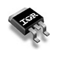
IRSF3010STR International Rectifier, IRSF3010STR Datasheet - Page 10

IRSF3010STR
Manufacturer Part Number
IRSF3010STR
Description
Manufacturer
International Rectifier
Datasheet
1.IRSF3010STR.pdf
(11 pages)
Specifications of IRSF3010STR
Power Switch Family
IRSF3010
Input Voltage
-0.3 to 10V
Power Switch On Resistance
85mOhm
Number Of Outputs
Single
Mounting
Surface Mount
Supply Current
350uA
Package Type
SMD-220
Pin Count
2 +Tab
Power Dissipation
40W
Lead Free Status / Rohs Status
Not Compliant
Application Information
Introduction
Protected monolithic POWER MOSFETs offer simple,
cost effective solutions in applications where extreme
operating conditions can occur. The margin between
the operating conditions and the absolute maxi-
mum values can be narrowed resulting in better
utilization of the device and lower cost. ESD protec-
tion also reduces the off-circuit failures during han-
dling and assembly.
General Description
The IRSF3010 is a fully protected monolithic N-chan-
nel, logic level POWER MOSFET with 80m
on-resistance. The built-in protections include over-
current, over-temperature, ESD and active over-volt-
age protections.
The over-current and over-temperature protection
makes the IRSF3010 indestructible at any load condi-
tions in switching or in linear applications. The built-in
ESD protection minimizes the risk of ESD damage
when the device is off-circuit. The IRSF3010 is fully
characterized for avalanche operation and can be used
for fast de-energization of inductive loads.
The IRSF3010 Intelligent Power Switch that is
available in the TO220 package offers an easy up-
grade from non-protected devices.
10
Fig.20 Block Diagram
(max)
Block Diagram
The zener diode between the input and the source
(see figure 20) provides the ESD protection for the
input and also limits the applicable voltage to the in-
put to 10V.
The R-S flip-flop memorizes the occurrence of an er-
ror condition and controls the Q2 and Q3 switches.
The flip-flop can be cleared by holding the input low
for the specified minimum duration.
COMP1 and COMP2 comparators are used to com-
pare the over-current and over-temperature signals
with the built-in reference. Either comparator can re-
set the fault flip-flop and turn Q1 off. During fault con-
dition, Q2 disconnects gate of Q1 from the input, Q3
shorts the gate and source of Q1, resulting in rapid
turn-off of Q1. The zener diode between the gate and
drain of Q1 turns Q1 on, when the drain to source
voltage exceeds 55V.
Switching Characteristics
In the IRSF3010 the control logic and the protection
circuits are powered from the input pin. When posi-
tive voltage appears at the input pin the R-S flip-flop
turns Q2 on and connects the gate of the main device
to the input.
The turn-on speed is limited by the channel resistance
of Q2 and the gate charge requirements of Q1. The
typical switching waveforms at 5V input voltage are
shown in figure 21. Using higher input voltage will
improve the turn-on time but it does not affect the turn-
off switching speed.
Fig.21 Waveforms switching clamped indictive
load using 5V input voltage
Input voltage 5V/
Time: 1 sV/div.
Drain voltage 5V/
Drain Current: 1A/div.


