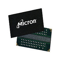
MT47H32M16BN-3:D Micron Technology Inc, MT47H32M16BN-3:D Datasheet - Page 60

MT47H32M16BN-3:D
Manufacturer Part Number
MT47H32M16BN-3:D
Description
Manufacturer
Micron Technology Inc
Type
DDR2 SDRAMr
Datasheet
1.MT47H32M16BN-3D.pdf
(139 pages)
Specifications of MT47H32M16BN-3:D
Organization
32Mx16
Density
512Mb
Address Bus
15b
Access Time (max)
450ps
Maximum Clock Rate
667MHz
Operating Supply Voltage (typ)
1.8V
Package Type
FBGA
Operating Temp Range
0C to 85C
Operating Supply Voltage (max)
1.9V
Operating Supply Voltage (min)
1.7V
Supply Current
250mA
Pin Count
84
Mounting
Surface Mount
Operating Temperature Classification
Commercial
Lead Free Status / Rohs Status
Compliant
Available stocks
Company
Part Number
Manufacturer
Quantity
Price
Company:
Part Number:
MT47H32M16BN-3:D
Manufacturer:
MICRON
Quantity:
2 526
Part Number:
MT47H32M16BN-3:D
Manufacturer:
MICRON
Quantity:
20 000
Company:
Part Number:
MT47H32M16BN-3:D TR
Manufacturer:
Micron Technology Inc
Quantity:
10 000
Part Number:
MT47H32M16BN-3:D(D9GMG)
Manufacturer:
MICRON
Quantity:
20 000
Input Slew Rate Derating
PDF: 09005aef82f1e6e2
Rev. M 9/08 EN
For all input signals, the total
by adding the data sheet
value, respectively. Example:
t
crossing of Vref(DC) and the first crossing of Vih(AC) MIN. Setup nominal slew rate (
for a falling signal is defined as the slew rate between the last crossing of Vref(DC) and
the first crossing of Vil(AC) MAX.
If the actual signal is always earlier than the nominal slew rate line between shaded
“Vref(DC) to AC region,” use the nominal slew rate for the derating value (Figure 26
(page 63)).
If the actual signal is later than the nominal slew rate line anywhere between the sha-
ded “Vref(DC) to AC region,” the slew rate of a tangent line to the actual signal from the
AC level to DC level is used for the derating value (see Figure 27 (page 63)).
t
crossing of Vil(DC) MAX and the first crossing of Vref(DC).
falling signal, is defined as the slew rate between the last crossing of Vih(DC) MIN and
the first crossing of Vref(DC).
If the actual signal is always later than the nominal slew rate line between shaded “DC
to Vref(DC) region,” use the nominal slew rate for the derating value (Figure 28
(page 64)).
If the actual signal is earlier than the nominal slew rate line anywhere between shaded
“DC to Vref(DC) region,” the slew rate of a tangent line to the actual signal from the DC
level to Vref(DC) level is used for the derating value (Figure 29 (page 65)).
Although the total setup time might be negative for slow slew rates (a valid input signal
will not have reached Vih[AC]/Vil[AC] at the time of the rising clock transition), a valid
input signal is still required to complete the transition and reach Vih(AC)/Vil(AC).
For slew rates in between the values listed in Table 28 (page 61) and Table 29
(page 62), the derating values may obtained by linear interpolation.
IS, the nominal slew rate for a rising signal, is defined as the slew rate between the last
IH, the nominal slew rate for a rising signal, is defined as the slew rate between the last
t
IS (base) and
t
60
t
IS (total setup time) =
IS (setup time) and
t
Micron Technology, Inc. reserves the right to change products or specifications without notice.
IH (base) value to the Δ
512Mb: x4, x8, x16 DDR2 SDRAM
t
IH (hold time) required is calculated
t
IS (base) + Δ
Input Slew Rate Derating
t
IH, nominal slew rate for a
© 2004 Micron Technology, Inc. All rights reserved.
t
IS and Δ
t
IS.
t
IH derating
t
IS)


