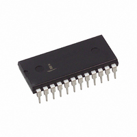
HI1-565ATD-2 Intersil, HI1-565ATD-2 Datasheet - Page 5

HI1-565ATD-2
Manufacturer Part Number
HI1-565ATD-2
Description
CONV D/A 12BIT 6.7MHZ 24-DIP
Manufacturer
Intersil
Datasheet
1.HI1-565AJD-5.pdf
(9 pages)
Specifications of HI1-565ATD-2
Number Of Bits
12
Data Interface
Parallel
Number Of Converters
1
Voltage Supply Source
Dual ±
Power Dissipation (max)
250mW
Operating Temperature
-55°C ~ 125°C
Mounting Type
Through Hole
Package / Case
24-DIP (0.600", 15.24mm)
Lead Free Status / RoHS Status
Lead free / RoHS Compliant
Settling Time
-
Available stocks
Company
Part Number
Manufacturer
Quantity
Price
added to convert this current to a voltage. Refer to Table 2
for the voltage output case, along with Figure 1 or Figure 2.
Calibration is a two step process for each of the five output
ranges shown in Table 2. First adjust the negative full scale
(zero for unipolar ranges). This is an offset adjust which
translates the output characteristic, i.e., affects each code by
the same amount.
Unipolar
(See Figure 1)
Bipolar
(See Figure 2)
MODE
100Ω
REF
R2
GND
IN
REF
0 to +10V
PRANGE
OUTPUT
0 to +5V
REF OUT
±2.5V
±10V
6
5
±5V
19.95K
5
+
-
4
V CC
10V
3
3.5K
PIN 10 TO
3K
CIRCUIT CONNECTIONS
TABLE 2. OPERATING MODES AND CALIBRATION
NC
V
V
V
V
0.5mA
O
O
O
O
I REF
-V
HI-565A
FIGURE 1. UNIPOLAR VOLTAGE OUTPUT
EE
+
-
7
PWR
GND
12
MSB
PIN 11 TO
24
CODE
INPUT
Pin 10
Pin 10
Pin 9
Pin 9
(4 x I REF
DAC
V
x CODE)
O
13
9.95K
OFF.
LSB
BIP.
I O
8
2.5K
RESlSTOR (R)
5K
5K
Next adjust positive FS. This is a gain error adjustment, which
rotates the output characteristic about the negative FS value.
For the bipolar ranges, this approach leaves an error at the
zero code, whose maximum value is the same as for integral
nonlinearity error. In general, only two values of output may
be calibrated exactly; all others must tolerate some error.
Choosing the extreme end points (plus and minus full scale)
minimizes this distributed error for all other codes.
1.43K
1.69K
1.43K
1.1K
1.1K
11
10
9
DAC
OUT
20V SPAN
10V SPAN
R (SEE
+
-
INPUT CODE
TABLE 2)
C
APPLY
All 0’s
All 1’s
All 0’s
All 1’s
All 0’s
All 1’s
All 0’s
All 1’s
All 0’s
All 1’s
V O
100Ω
100kΩ
CALIBRATION
ADJUST
R1
R2
R1
R2
R3
R4
R3
R4
R3
R4
R1
50kΩ
+15V
-15V
+9.99756V
+4.99878V
+9.99512V
+4.99756V
+2.49878V
TO SET
-2.5V
-10V
-5V
V
0V
0V
O


