HI5960IAZ Intersil, HI5960IAZ Datasheet - Page 3
HI5960IAZ
Manufacturer Part Number
HI5960IAZ
Description
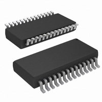
CONV D/A 14BIT 130MSPS 28-TSSOP
Manufacturer
Intersil
Datasheet
1.HI5960IBZ.pdf
(12 pages)
Specifications of HI5960IAZ
Settling Time
35ns
Number Of Bits
14
Data Interface
Parallel
Number Of Converters
1
Voltage Supply Source
Analog and Digital
Power Dissipation (max)
200mW
Operating Temperature
-40°C ~ 85°C
Mounting Type
Surface Mount
Package / Case
28-TSSOP
Lead Free Status / RoHS Status
Lead free / RoHS Compliant
Available stocks
Company
Part Number
Manufacturer
Quantity
Price

Part Number:
HI5960IAZ
Manufacturer:
INTERSIL
Quantity:
20 000


Pin Descriptions
PIN NO.
20, 25
1-14
15
16
17
18
19
21
22
23
24
26
27
28
D13 (MSB) Through
PIN NAME
D0 (LSB)
COMP1
COMP2
REFLO
SLEEP
FSADJ
REFIO
IOUTB
IOUTA
DCOM
ACOM
AV
DV
CLK
DD
DD
3
Digital Data Bit 13, (Most Significant Bit) through Digital Data Bit 0, (Least Significant Bit).
Control Pin for Power-Down mode. Sleep Mode is active high; Connect to ground for Normal Mode. Sleep
pin has internal 20µA active pulldown current.
Connect to analog ground to enable internal 1.2V reference or connect to AV
reference.
Reference voltage input if internal reference is disabled. Reference voltage output if internal reference is
enabled. Use 0.1µF cap to ground when internal reference is enabled.
Full Scale Current Adjust. Use a resistor to ground to adjust full scale output current. Full Scale Output
Current = 32 x V
For use in reducing bandwidth/noise. Recommended: connect 0.1µF to AV
The complimentary current output of the device. Full scale output current is achieved when all input bits
are set to binary 0.
Current output of the device. Full scale output current is achieved when all input bits are set to binary 1.
Connect 0.1µF capacitor to ACOM.
Analog Supply (+3V to +5V).
Connect to Analog Ground.
Connect to Digital Ground.
Digital Supply (+3V to +5V).
Clock Input. Input data to the DAC passes through the “master” latches when the clock is low and is
latched into the “master” latches when the clock is high. Data presented to the “slave” latch passes
through when the clock is logic high and is latched into the “slave” latches when the clock is logic low.
Adequate setup time must be allowed for the MSBs to pass through the thermometer decoder before the
clock goes high. This master-slave arrangement comprises an edge-triggered flip-flop, with the DAC
being updated on the rising clock edge. It is recommended that the clock edge be skewed such that setup
time is larger than the hold time.
FSADJ
/R
SET
HI5960
.
DESCRIPTION
DD
DD
.
to disable internal
Related parts for HI5960IAZ
Image
Part Number
Description
Manufacturer
Datasheet
Request
R

Part Number:
Description:
14-bit, 130msps, Commlink? High Speed D/a Converter
Manufacturer:
Intersil Corporation
Datasheet:
Part Number:
Description:
Intersil Corporation [CMOS Serial Controller Interface]
Manufacturer:
Intersil Corporation
Datasheet:
Part Number:
Description:
Manufacturer:
Intersil Corporation
Datasheet:
Part Number:
Description:
357-036-542-201 CARDEDGE 36POS DL .156 BLK LOPRO
Manufacturer:
Intersil Corporation
Datasheet:
Part Number:
Description:
1024-Word x 4-Bit LSI Static RAM
Manufacturer:
Intersil Corporation
Datasheet:
Part Number:
Description:
General Purpose NPN Transistor Arrays FN341.4
Manufacturer:
Intersil Corporation
Datasheet:
Part Number:
Description:
CMOS 16-Bit Microprocessor
Manufacturer:
Intersil Corporation
Datasheet:
Part Number:
Description:
Manufacturer:
Intersil Corporation
Datasheet:
Part Number:
Description:
Manufacturer:
Intersil Corporation
Datasheet:
Part Number:
Description:
Manufacturer:
Intersil Corporation
Datasheet:
Part Number:
Description:
Manufacturer:
Intersil Corporation
Datasheet:
Part Number:
Description:
CMOS 6-Bit Latch and Decoder Memory Interfaces
Manufacturer:
Intersil Corporation
Datasheet:
Part Number:
Description:
CA3046General Purpose NPN Transistor Arrays
Manufacturer:
Intersil Corporation
Datasheet:
Part Number:
Description:
Manufacturer:
Intersil Corporation
Datasheet:
Part Number:
Description:
TR909 DLC/FLC SLIC with Low Power Standby
Manufacturer:
Intersil Corporation
Datasheet: