HI5660/6IA Intersil, HI5660/6IA Datasheet - Page 5
HI5660/6IA
Manufacturer Part Number
HI5660/6IA
Description
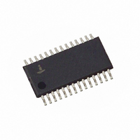
IC DAC 8-BIT 60MSPS 28-TSSOP
Manufacturer
Intersil
Datasheet
1.HI56606IAZ.pdf
(9 pages)
Specifications of HI5660/6IA
Settling Time
15ns
Number Of Bits
8
Data Interface
Parallel
Number Of Converters
1
Voltage Supply Source
Analog and Digital
Power Dissipation (max)
165mW
Operating Temperature
-40°C ~ 85°C
Mounting Type
Surface Mount
Package / Case
28-TSSOP
Lead Free Status / RoHS Status
Contains lead / RoHS non-compliant
Available stocks
Company
Part Number
Manufacturer
Quantity
Price
Company:

Part Number:
HI5660/6IA
Manufacturer:
Intersil
Quantity:
96
Company:
Part Number:
HI5660/6IAZ
Manufacturer:
Intersil
Quantity:
450


Electrical Specifications
NOTES:
10. Measured with the clock at 60MSPS and the output frequency at 10MHz.
TIMING CHARACTERISTICS
Data Setup Time, t
Data Hold Time, t
Propagation Delay Time, t
CLK Pulse Width, t
POWER SUPPLY CHARACTERISTICS
AV
DV
Analog Supply Current (I
Digital Supply Current (I
Supply Current (I
Power Dissipation
Power Supply Rejection
2. Gain Error measured as the error in the ratio between the full scale output current and the current through R
3. Parameter guaranteed by design or characterization and not production tested.
4. Spectral measurements made with differential transformer coupled output and no external filtering.
5. Measured with the clock at 50MSPS and the output frequency at 1MHz.
6. Measured with the clock at 100MSPS and the output frequency at 40MHz.
7. See ‘Definition of Specifications’.
8. It is recommended that the output current be reduced to 12mA or less to maintain optimum performance for operation below 3V. DV
9. For operation above 125MHz, it is recommended that the power supply be 3.3V or greater. The part is functional with the clock above 125MSPS
DD
DD
ratio should be 32.
do not have to be equal .
and the power supply below 3.3V, but performance is degraded.
Power Supply
Power Supply
PARAMETER
AVDD
HLD
SU
PW1
) Sleep Mode
, t
DVDD
AVDD
PW2
PD
)
)
5
AV
DD
See Figure 3 (Note 3)
See Figure 3 (Note 3)
See Figure 3
See Figure 3 (Note 3)
(Note 8, 9)
(Note 8, 9)
5V or 3V, IOUTFS = 20mA
5V or 3V, IOUTFS = 2mA
5V, IOUTFS = Don’t Care (Note 5)
3V, IOUTFS = Don’t Care (Note 5)
5V or 3V, IOUTFS = Don’t Care
5V, IOUTFS = 20mA (Note 6)
5V, IOUTFS = 20mA (Note 10)
5V, IOUTFS = 2mA (Note 6)
3.3V, IOUTFS = 20mA (Note 10)
3V, IOUTFS = 20mA (Note 6)
3V, IOUTFS = 20mA (Note 10)
3V, IOUTFS = 2mA (Note 6)
Single Supply (Note 7)
= DV
DD
= +5V, V
REF
TEST CONDITIONS
= Internal 1.2V, IOUTFS = 20mA, T
HI5660
A
= 25
o
C for All Typical Values (Continued)
MIN
-0.2
2.7
2.7
T
3
3
4
-
-
-
-
-
-
-
-
-
-
-
-
-
A
SET
= -40
(typically 625µA). Ideally the
TYP
165
150
o
5.0
5.0
1.5
1.6
23
70
75
85
67
27
1
4
3
C TO 85
-
-
-
-
MAX
+0.2
5.5
5.5
o
30
5
3
-
-
-
-
-
-
-
-
-
-
-
-
-
C
DD
and AV
% FSR/V
UNITS
mW
mW
mW
mW
mW
mW
mW
mA
mA
mA
mA
mA
ns
ns
ns
ns
V
V
DD
Related parts for HI5660/6IA
Image
Part Number
Description
Manufacturer
Datasheet
Request
R

Part Number:
Description:
CONV D/A 8-BIT 60MSPS 28-TSSOP
Manufacturer:
Intersil
Datasheet:
Part Number:
Description:
CONV D/A 8-BIT 60MSPS 28-TSSOP
Manufacturer:
Intersil
Datasheet:

Part Number:
Description:
8-Bit, 165/125/60MSPS, High Speed D/A Converter
Manufacturer:
INTERSIL [Intersil Corporation]
Datasheet:
Part Number:
Description:
CONV D/A 8-BIT 60MSPS 28-TSSOP
Manufacturer:
Intersil
Datasheet:

Part Number:
Description:
8-bit, 165/125/60msps, High Speed D/a Converter
Manufacturer:
Intersil Corporation
Datasheet:
Part Number:
Description:
Intersil Corporation [CMOS Serial Controller Interface]
Manufacturer:
Intersil Corporation
Datasheet:
Part Number:
Description:
Manufacturer:
Intersil Corporation
Datasheet:
Part Number:
Description:
357-036-542-201 CARDEDGE 36POS DL .156 BLK LOPRO
Manufacturer:
Intersil Corporation
Datasheet:
Part Number:
Description:
1024-Word x 4-Bit LSI Static RAM
Manufacturer:
Intersil Corporation
Datasheet:
Part Number:
Description:
General Purpose NPN Transistor Arrays FN341.4
Manufacturer:
Intersil Corporation
Datasheet:
Part Number:
Description:
CMOS 16-Bit Microprocessor
Manufacturer:
Intersil Corporation
Datasheet:
Part Number:
Description:
Manufacturer:
Intersil Corporation
Datasheet:
Part Number:
Description:
Manufacturer:
Intersil Corporation
Datasheet:
Part Number:
Description:
Manufacturer:
Intersil Corporation
Datasheet:
Part Number:
Description:
Manufacturer:
Intersil Corporation
Datasheet: