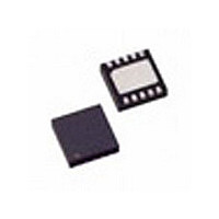
LTC2919HDDB-5#PBF Linear Technology, LTC2919HDDB-5#PBF Datasheet - Page 7

LTC2919HDDB-5#PBF
Manufacturer Part Number
LTC2919HDDB-5#PBF
Description
Manufacturer
Linear Technology
Datasheet
1.LTC2919HDDB-5PBF.pdf
(16 pages)
Specifications of LTC2919HDDB-5#PBF
Voltage Supervisor Type
Voltage Monitor
Number Of Voltage Supervisors
2
Monitored Supervisor Voltage
3.3
Operating Supply Voltage (min)
0.5V
Operating Temperature Classification
Automotive
Operating Temp Range
-40C to 125C
Pin Count
10
Mounting
Surface Mount
Lead Free Status / Rohs Status
Compliant
Available stocks
Company
Part Number
Manufacturer
Quantity
Price
BLOCK DIAGRA
TI I G DIAGRA S
PI FU CTIO S
ADJ1 (Pin 10): Adjustable Voltage Input 1. Input to volt-
age monitor comparator 1 (0.5V nominal threshold). The
polarity of the input is selected by the state of the SEL
pin (refer to Table 1). Tie to REF if unused (with SEL =
V
CC
W
U
or Open).
U
U
U
W
(MSOP/DFN Package)
W
Positive Polarity Input Timing
Negative Polarity Input Timing
UVLO Timing
NOTES:
1. ΔV
2. IN COMPARATOR MODE, t
Comparator Mode
ADJ1
ADJ2
REF
V
RT
CC
AND ΔV
+
–
500mV
CC(UVLO)
+
–
+
–
+
–
CONTROL 2
= 0, except in
RST
+
–
THREE-STATE
= t
DECODE
PROP
SEL
.
CONTROL 1
EN
+
–
1.000V
V
V
RST
OUT
RST
OUT
RST
OUT
V
ADJ
ADJ
CC
V
t
t
t
PROP
PROP
PROP
CC(UVLO)
V
V
RT
RT
1V
1V
1V
1V
1V
1V
CONTROL = H = NEGATIVE POLARITY
CONTROL = L = POSITIVE POLARITY
OPEN
GND
SEL
V
Exposed Pad (Pin 11, DFN Only): The Exposed Pad may
be left unconnected. For better thermal contact, tie to a PCB
trace. This trace must be grounded or unconnected.
CC
t
t
t
PROP
PROP
UV
CONTROL 1
ADJUSTABLE
GENERATOR
GENERATOR
PULSE
200ms
PULSE
H
L
L
V
V
V
V
RT
RT
CC
CC(UVLO)
6.5V
+ ΔV
– ΔV
V
t
t
PROP
PROP
CC
t
PROP
RT
RT
t
t
t
CONTROL 2
RST
RST
RST
+ ΔV
CC(UVLO)
H
H
L
THREE-STATE
DECODE
2919 TD
OUT1
OUT2
TMR
GND
RST
2919 BD
LTC2919
7
2919f


