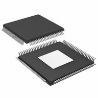
AD9787BSVZ Analog Devices Inc, AD9787BSVZ Datasheet - Page 32

AD9787BSVZ
Manufacturer Part Number
AD9787BSVZ
Description
IC DAC 14BIT 800MSPS 100TQFP
Manufacturer
Analog Devices Inc
Series
TxDAC®r
Datasheet
1.AD9785BSVZ.pdf
(64 pages)
Specifications of AD9787BSVZ
Data Interface
Serial
Number Of Bits
14
Number Of Converters
2
Voltage Supply Source
Analog and Digital
Power Dissipation (max)
450mW
Operating Temperature
-40°C ~ 85°C
Mounting Type
Surface Mount
Package / Case
100-TQFP Exposed Pad, 100-eTQFP, 100-HTQFP, 100-VQFP
Resolution (bits)
14bit
Sampling Rate
800MSPS
Input Channel Type
Parallel
Digital Ic Case Style
QFP
No. Of Pins
100
Operating Temperature Range
-40°C To +85°C
Lead Free Status / RoHS Status
Lead free / RoHS Compliant
Settling Time
-
Lead Free Status / RoHS Status
Lead free / RoHS Compliant, Lead free / RoHS Compliant
Available stocks
Company
Part Number
Manufacturer
Quantity
Price
Company:
Part Number:
AD9787BSVZ
Manufacturer:
ADI
Quantity:
200
Company:
Part Number:
AD9787BSVZ
Manufacturer:
Analog Devices Inc
Quantity:
10 000
Company:
Part Number:
AD9787BSVZRL
Manufacturer:
Analog Devices Inc
Quantity:
10 000
AD9785/AD9787/AD9788
The frequency tuning word (FTW) register comprises four bytes located at Address 0x0A.
Table 20. Frequency Tuning Word (FTW) Register
Address
0x0A
The phase control register (PCR) comprises four bytes located at Address 0x0B.
Table 21. Phase Control Register (PCR)
Address
0x0B
The amplitude scale factor (ASF) register comprises three bytes located at Address 0x0C.
Table 22. Amplitude Scale Factor (ASF) Register
Address
0x0C
The output offset (OOF) register comprises four bytes located at Address 0x0D.
Table 23. Output Offset (OOF) Register
Address
0x0D
The version register (VR) comprises two bytes located at Address 0x0E and is read only.
Table 24. Version Register (VR)
Address
0x0E
[31:0]
Bit
[31:26]
[25:16]
[15:0]
[31:16]
[15:0]
Bit
Bit
[23:18]
[17:9]
[8:0]
Bit
Bit
[15:8]
[7:0]
Name
Frequency Tuning
Word [31:0]
Name
Q DAC Offset [15:0]
I DAC Offset [15:0]
Reserved
Phase Correction
Word [9:0]
NCO Phase Offset
Word [15:0]
Name
Name
Reserved
Q DAC Amplitude
Scale Factor [8:0]
I DAC Amplitude
Scale Factor [8:0]
Name
Reserved
Version ID
Description
These bits are the 16-bit Q DAC offset factor. The LSB bit weight is 2
These bits are the 16-bit I DAC offset factor. The LSB bit weight is 2
Description
Reserved for future use.
These bits are the 9-bit Q DAC amplitude scale factor. The bit weighting is MSB = 2
LSB = 2
1.0 (0x080), the gain block is bypassed. This changes the latency of the signal. Therefore, in
systems using quadrature signals, either both I and Q scale factors should be bypassed or
both should have gains set to a value other than 1.0.
These bits are the 9-bit I DAC amplitude scale factor. The bit weighting is MSB = 2
LSB = 2
Description
Reserved for future use.
These bits read back the current version of the product.
Description
These bits make up the frequency tuning word applied to the NCO phase accumulator.
See the Numerically Controlled Oscillator section for details.
Description
Reserved for future use.
These bits are the 10-bit phase correction word.
These bits are the 16-bit NCO phase offset word. See the Numerically Controlled Oscillator
section for details.
−7
−7
, which yields a multiplier range of 0 to 3.9921875. Note that by setting the gain to
, which yields a multiplier range of 0 to 3.9921875.
Rev. A | Page 32 of 64
0
.
0
.
1
,
1
,


