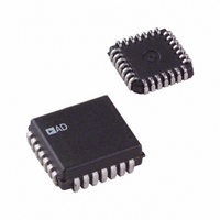
AD7225LP Analog Devices Inc, AD7225LP Datasheet - Page 10

AD7225LP
Manufacturer Part Number
AD7225LP
Description
IC DAC 8BIT QUAD W/AMP 28-PLCC
Manufacturer
Analog Devices Inc
Datasheet
1.AD7225CRSZ.pdf
(24 pages)
Specifications of AD7225LP
Rohs Status
RoHS non-compliant
Settling Time
4µs
Number Of Bits
8
Number Of Converters
4
Voltage Supply Source
Dual ±
Power Dissipation (max)
500mW
Operating Temperature
-40°C ~ 85°C
Mounting Type
Surface Mount
Package / Case
28-LCC (J-Lead)
Data Interface
-
Available stocks
Company
Part Number
Manufacturer
Quantity
Price
Part Number:
AD7225LP
Manufacturer:
ADI/亚德诺
Quantity:
20 000
Company:
Part Number:
AD7225LP-REEL
Manufacturer:
Analog Devices Inc
Quantity:
10 000
Company:
Part Number:
AD7225LPZ
Manufacturer:
Analog Devices Inc
Quantity:
10 000
Part Number:
AD7225LPZ
Manufacturer:
ADI/亚德诺
Quantity:
20 000
AD7225
INTERFACE LOGIC INFORMATION
The AD7225 contains two registers per DAC, an input register
and a DAC register. The A0 and A1 address lines select which
input register accepts data from the input port. When the WR
signal is low, the input latches of the selected DAC are transpa-
rent. The data is latched into the addressed input register on the
rising edge of
registers on the AD7225.
Table 5. AD7225 Addressing
A1
Low
Low
High
High
Only the data held in the DAC register determines the analog
output of the converter. The LDAC signal is common to all four
DACs and controls the transfer of information from the input
registers to the DAC registers. Data is latched into all four DAC
registers simultaneously on the rising edge of LDAC . The LDAC
signal is level triggered and therefore the DAC registers can be
made transparent by tying LDAC low (in this case, the outputs
of the converters respond to the data held in their respective
input latches). LDAC is an asynchronous signal and is indepen-
dent of WR . This is useful in many applications. However, in
systems where the asynchronous LDAC can occur during a
write cycle (or vice versa), care must be taken to ensure that
incorrect data is not latched through to the output. If LDAC is
activated prior to the rising edge of WR (or WR occurs during
LDAC ), LDAC must stay low for t
to ensure correct data is latched through to the output. Table 6
shows the truth table for AD7225 operation. Figure 12 shows
the input control logic for the part; the write cycle timing
diagram is given in Figure 13.
Table 6. Truth Table
WR
High
Low
High
High
Low
LDAC
High
High
High
Low
Low
A0
Low
High
Low
High
WR .
Function
No operation. Device not selected.
Input register of selected DAC transparent.
Input register of selected DAC latched.
All four DAC registers Transparent (that is,
outputs respond to data held in respective
input registers). Input registers are latched.
All four DAC registers latched.
DAC registers and selected input register
transparent output follows input data for
selected channel.
Table 5
Selected Input Register
DAC A
DAC B
DAC C
DAC D
shows the addressing for the input
6
or longer after WR
goes high
Rev. C | Page 10 of 24
LDAC
ADDRESS
NOTES
1. ALL INPUT SIGNAL RISE AND FALL TIMES MEASURED FROM
2. TIMING MEASUREMENT REFERENCE LEVEL IS
3. IF LDAC IS ACTIVATED PRIOR TO THE RISING EDGE OF WR,
WR
DATA IN
10% TO 90% OF 5V.
THEN IT MUST STAY LOW FOR
GOES HIGH.
A0
A1
LDAC
t
V
R
INH
WR
=
t
+ V
2
F
t
= 20ns OVER V
2
INL
V
V
INH
INL
Figure 13. Write Cycle Timing Diagram
t
1
Figure 12. Input Control Logic
DD
t
VALID
DATA
4
RANGE.
t
t
5
6
t
OR LONGER AFTER WR
3
TO ALL
DAC LATCHES
TO INPUT
LATCH A
TO INPUT
LATCH B
TO INPUT
LATCH C
TO INPUT
LATCH D
t
6
5V
0V
5V
5V
5V
0V


