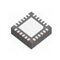
LM48511SQ National Semiconductor, LM48511SQ Datasheet - Page 17

LM48511SQ
Manufacturer Part Number
LM48511SQ
Description
Manufacturer
National Semiconductor
Datasheet
1.LM48511SQ.pdf
(22 pages)
Specifications of LM48511SQ
Operational Class
Class-D
Audio Amplifier Output Configuration
1-Channel Mono
Output Power (typ)
6.7x1@4OhmW
Audio Amplifier Function
Speaker
Single Supply Voltage (typ)
Not RequiredV
Dual Supply Voltage (typ)
5V
Power Supply Requirement
Triple
Rail/rail I/o Type
No
Power Supply Rejection Ratio
88dB
Single Supply Voltage (min)
Not RequiredV
Single Supply Voltage (max)
Not RequiredV
Dual Supply Voltage (min)
3/4.8V
Dual Supply Voltage (max)
5.5/8V
Operating Temp Range
-40C to 85C
Operating Temperature Classification
Industrial
Mounting
Surface Mount
Pin Count
24
Lead Free Status / Rohs Status
Not Compliant
Available stocks
Company
Part Number
Manufacturer
Quantity
Price
Part Number:
LM48511SQ
Manufacturer:
TI/德州仪器
Quantity:
20 000
Company:
Part Number:
LM48511SQ/NOPB
Manufacturer:
VTI
Quantity:
1 928
Company:
Part Number:
LM48511SQX/NOPB
Manufacturer:
NSC
Quantity:
1 720
Where R
R
CALCULATING REGULATOR OUTPUT CURRENT
The load current of the boost converter is related to the av-
erage inductor current by the relation:
Where "DC" is the duty cycle of the application.
The switch current can be found by:
Inductor ripple current is dependent on inductance, duty cy-
cle, supply voltage and frequency:
FB3
is given by:
I
SW
CO
I
AMP
= I
is the ESR of the output capacitor. The value of
= I
INDUCTOR(AVE)
INDUCTOR(AVE)
R4 =1 / 2
π
+ 1/2 (I
f
CO
x (1 - DC) (A)
C1
RIPPLE
) (A)
(11)
(12)
(13)
17
where f = switching frequency = 1MHz
combining all terms, we can develop an expression which al-
lows the maximum available load current to be calculated:
The equation shown to calculate maximum load current takes
into account the losses in the inductor or turn-off switching
losses of the FET and diode.
DESIGN PARAMETERS V
The value of the FET "ON" voltage (referred to as V
equations 9 thru 12) is dependent on load current. A good
approximation can be obtained by multiplying the on resis-
tance (R
The maximum peak switch current the device can deliver is
dependent on duty cycle.
I
AMP(max)
DS(ON)
I
RIPPLE
= (1–DC)x[I
of the FET times the average inductor current.
= DC x (V
SW(max)
DD
SW
-V
SW
–DC(V-V
AND I
) / (f x L) (A)
SW
SW
)]/2fL (A)
www.national.com
SW
(14)
(15)
in


