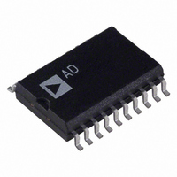
AD7849CR Analog Devices Inc, AD7849CR Datasheet - Page 7

AD7849CR
Manufacturer Part Number
AD7849CR
Description
IC DAC 16BIT SRL INP 20-SOIC
Manufacturer
Analog Devices Inc
Datasheet
1.AD7849BRZ.pdf
(20 pages)
Specifications of AD7849CR
Rohs Status
RoHS non-compliant
Settling Time
7µs
Number Of Bits
16
Data Interface
Serial
Number Of Converters
1
Voltage Supply Source
Analog and Digital, Dual ±
Power Dissipation (max)
100mW
Operating Temperature
-40°C ~ 85°C
Mounting Type
Surface Mount
Package / Case
20-SOIC (7.5mm Width)
Available stocks
Company
Part Number
Manufacturer
Quantity
Price
Company:
Part Number:
AD7849CRZ
Manufacturer:
CYPRESS
Quantity:
5 560
Part Number:
AD7849CRZ
Manufacturer:
ADI/亚德诺
Quantity:
20 000
PIN CONFIGURATION AND FUNCTION DESCRIPTIONS
Table 6. Pin Function Descriptions
Pin No.
1
2
3
4
5
6
7
8
9
10
11
12
13
14
15
16
17
18
19
20
SCLK
DGND
SDIN
AGND
NC
Mnemonic
V
V
V
SYNC
V
SDOUT
DCEN
BIN/COMP
LDAC
CLR
RSTIN
RSTOUT
V
V
R
REF+
REF−
SS
CC
DD
OUT
OFS
Description
V
V
Negative supply for the analog circuitry. This is nominally –15 V.
Data Synchronization Logic Input. When it goes low, the internal logic is initialized in readiness for a new data-word.
Serial Clock Logic Input. Data is clocked into the input register on each SCLK falling edge.
Positive supply for the digital circuitry. This is nominally 5 V.
Serial Data Output. With DCEN at Logic 1, this output is enabled, and the serial data in the input shift register is
clocked out on each rising edge of SCLK.
Daisy-Chain Enable Logic Input. Connect this pin high if a daisy-chain interface is being used; otherwise, this
pin must be connected low.
Logic Input. This input selects the data format to be either binary or twos complement. In the unipolar output
range, natural binary format is selected by connecting the input to Logic 0. In the bipolar output range, offset
binary is selected by connecting this input to Logic 0, and twos complement is selected by connecting it to a
Logic 1.
Digital Ground. Ground reference point for the on-chip digital circuitry.
Load DAC Logic Input. This input updates the DAC output. The DAC output is updated on the falling edge of
this signal, or alternatively, if this input is permanently low, an automatic update mode is selected where the
DAC is updated on the 16th falling SCLK edge.
Serial Data Input. The 16-bit serial data-word is applied to this input.
Clear Logic Input. Taking this input low sets V
complement output range. It sets V
Reset Logic Input. This input allows external access to the internal reset logic. Applying Logic 0 to this input,
resets the DAC output to 0 V. In normal operation, it should be tied to Logic 1.
Reset Logic Output. This is the output from the on-chip voltage monitor used in the reset circuit. It can be used
to control other system components, if desired.
This is the analog ground for the device. It is the point to which the output gets shorted in reset mode.
Positive Supply for the Analog Circuitry. This is 15 V nominal.
No Connect. Leave unconnected.
DAC Output Voltage Pin.
Input to Summing Resistor of DAC Output Amplifier. This is used to select the output voltage ranges. Also, see
Figure 20 to Figure 23 in the Applying the AD7849 section.
REF+
REF−
Input. The DAC is specified for V
Input. The DAC is specified for V
NC = NO CONNECT. DO NOT CONNECT TO THIS PIN.
BIN/COMP
SDOUT
DGND
V
V
SYNC
DCEN
SCLK
REF+
REF–
V
V
CC
SS
Figure 2. Pin Configuration
10
1
2
3
4
5
6
7
8
9
Rev. C | Page 7 of 20
(Not to Scale)
OUT
AD7849
TOP VIEW
REF+
REF−
to V
of 5 V. The DAC is fully multiplying so that the V
of –5 V. The DAC is fully multiplying so that the V
REF–
OUT
in the offset binary bipolar output range.
20
19
18
17
16
15
14
13
12
11
to 0 V in both the unipolar output range and the bipolar twos
R
V
NC
V
AGND
RSTOUT
RSTIN
CLR
SDIN
LDAC
OUT
DD
OFS
REF+
REF−
range is +5 V to –5 V.
range is –5 V to +5 V.
AD7849


