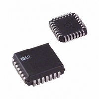
AD767KP Analog Devices Inc, AD767KP Datasheet - Page 8

AD767KP
Manufacturer Part Number
AD767KP
Description
IC DAC 12BIT W/AMP 28-PLCC
Manufacturer
Analog Devices Inc
Datasheet
1.AD767JNZ.pdf
(8 pages)
Specifications of AD767KP
Data Interface
Parallel
Rohs Status
RoHS non-compliant
Settling Time
3µs
Number Of Bits
12
Number Of Converters
1
Voltage Supply Source
Dual ±
Operating Temperature
0°C ~ 70°C
Mounting Type
Surface Mount
Package / Case
28-LCC (J-Lead)
Resolution (bits)
12bit
Sampling Rate
500kSPS
Input Channel Type
Parallel
Supply Current
18mA
Digital Ic Case Style
LCC
No. Of Pins
25
Power Dissipation (max)
-
Lead Free Status / RoHS Status
Contains lead / RoHS non-compliant
Available stocks
Company
Part Number
Manufacturer
Quantity
Price
Part Number:
AD767KPZ
Manufacturer:
ADI/亚德诺
Quantity:
20 000
Company:
Part Number:
AD767KPZ-REEL
Manufacturer:
Analog Devices Inc
Quantity:
10 000
AD767
Figure 11. TMS320C25 – AD767 Interface
Figure 9. TMS32020 – AD767 Interface
ADSP-2100 – AD767 INTERFACE
OUTLINE DIMENSIONS
The ADSP-2100 single chip DSP processor may be interfaced
Dimensions shown in inches and (mm).
to the AD767 as shown in Figure 10. With a clock frequency of
32 MHz, and instruction execution in a single 125 ns cycle, the
24-Pin Ceramic (Suffix D)
processor will support the AD767 interface with a single wait
state.
24-Pin Plastic (Suffix N)
Figure 10. ADSP-2100 – AD767 Interface
At the beginning of the data memory access cycle the processor
provides a 14-bit address on the DMA bus. The DMS signal is
then asserted enabling a LOW address decode. Valid data is
now placed on the data bus and DMWR is issued. DMWR is
OR’ed with the LOW address decode to generate the AD767
CS.
The LOW decoded address is also gated with the Q output of a
D flip-flop to hold DMACK (Data Memory Acknowledge)
LOW. This forces the processor into a wait state and extends
28-Pin PLCC (Suffix P)
the AD767 CS by 1 clock cycle. The rising edge of CLKOUT
latches Q HIGH bringing DMACK HIGH. The cycle is now
complete.
TMS320C25 – AD767 INTERFACE
Figure 11 illustrates the AD767 interface to a TMS320C25
digital signal processor. Due to the high-speed capability of the
processor (40 MHz), a single wait state is required and is easily
generated using MSC. A 20 MHz TMS320C25 however, does
not require wait states and should be interfaced using the circuit
shown in Figure 9.
–8–
REV. A


