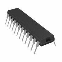
AD7225LNZ Analog Devices Inc, AD7225LNZ Datasheet - Page 6

AD7225LNZ
Manufacturer Part Number
AD7225LNZ
Description
IC DAC 8BIT LC2MOS QUAD 24-DIP
Manufacturer
Analog Devices Inc
Datasheet
1.AD7225CRSZ.pdf
(24 pages)
Specifications of AD7225LNZ
Settling Time
4µs
Number Of Bits
8
Number Of Converters
4
Voltage Supply Source
Dual ±
Power Dissipation (max)
500mW
Operating Temperature
-40°C ~ 85°C
Mounting Type
Through Hole
Package / Case
24-DIP (0.300", 7.62mm)
Resolution (bits)
8bit
Sampling Rate
200kSPS
Input Channel Type
Parallel
Supply Current
10mA
Digital Ic Case Style
DIP
No. Of Pins
24
Data Interface
CMOS, Parallel, TTL
Lead Free Status / RoHS Status
Lead free / RoHS Compliant
Available stocks
Company
Part Number
Manufacturer
Quantity
Price
AD7225
PIN CONFIGURATIONS AND FUNCTION DESCRIPTIONS
Table 4. Pin Function Descriptions
PDIP, SOIC,
CERDIP, SSOP
1
2
3
4
5
6
7
8
9
10
11
12
13
14
15
16
17
18
19
20
21
22
23
24
N/A
Pin No.
Figure 2. PDIP, SOIC, CERDIP, and SSOP
V
V
V
V
AGND
DGND
LDAC
OUT
OUT
REF
REF
DB7
DB6
DB5
DB4
V
SS
B
A
B
A
10
11
12
1
2
3
4
5
6
7
8
9
PLCC
2
3
4
5
6
7
9
10
11
12
13
14
16
17
18
19
20
21
23
24
25
26
27
28
1, 8, 15, 22
(Not to Scale)
AD7225
TOP VIEW
24
23
22
21
20
19
18
17
16
15
14
13
Mnemonic
V
V
V
V
V
AGND
DGND
LDAC
DB7
DB6
DB5
DB4
DB3
DB2
DB1
DB0
WR
A1
A0
V
V
V
V
V
NC
V
V
V
V
V
A0
A1
WR
DB0
DB1
DB2
DB3
OUT
OUT
DD
REF
REF
OUT
OUT
SS
REF
REF
REF
REF
DD
OUT
OUT
B
A
D
C
C
D
C
D
B
A
D
C
Description
DAC Channel B Voltage Output.
DAC Channel A Voltage Output.
Negative Power Supply Connection.
Reference Voltage Connection for DAC Channel B.
Reference Voltage Connection for DAC Channel A.
Analog Ground Reference Connection.
Digital Ground Reference Connection.
Active Low Load DAC Signal. DAC register data is latched on the rising edge of LDAC.
Data Bit 7 (Most Significant Data Bit).
Data Bit 6.
Data Bit 5.
Data Bit 4.
Data Bit 3.
Data Bit 2.
Data Bit 1.
Data Bit 0 (Least Significant Data Bit).
Active Low Data Write Signal. Input register data is latched on the rising edge of WR.
DAC Address Select Pin.
DAC Address Select Pin.
Reference Voltage Connection for DAC Channel D.
Reference Voltage Connection for DAC Channel C.
Positive Power Supply Connection.
DAC Channel D Voltage Output.
DAC Channel C Voltage Output.
No Internal Connection.
Rev. C | Page 6 of 24
V
V
AGND
DGND
LDAC
REF
REF
DB7
NC
B
A
10
11
5
6
7
8
9
12
4
INDENTFIER
NC = NO CONNECT
13 14
3
(Not to Scale)
Figure 3. PLCC
AD7225
TOP VIEW
PIN 1
2
15
1
16 17
28
27 26
18
19
25
24
23
22
21
20
V
V
A0
NC
A1
WR
DB0
REF
REF
C
D


