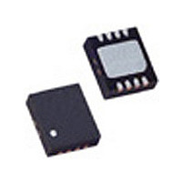
LTC2912IDDB-1#PBF Linear Technology, LTC2912IDDB-1#PBF Datasheet - Page 6

LTC2912IDDB-1#PBF
Manufacturer Part Number
LTC2912IDDB-1#PBF
Description
Manufacturer
Linear Technology
Datasheet
1.LTC2912IDDB-1PBF.pdf
(12 pages)
Specifications of LTC2912IDDB-1#PBF
Voltage Supervisor Type
Voltage Monitor
Number Of Voltage Supervisors
1
Monitored Supervisor Voltage
3.3
Reset Threshold Voltage (min)
AdjV
Reset Threshold Voltage (max)
AdjV
Operating Supply Voltage (min)
2.3V
Operating Supply Voltage (max)
6V
Operating Temperature Classification
Industrial
Operating Temp Range
-40C to 85C
Pin Count
8
Mounting
Surface Mount
Lead Free Status / Rohs Status
Compliant
Available stocks
Company
Part Number
Manufacturer
Quantity
Price
LTC2912
PIN FUNCTIONS
OV (Pin 6/Pin 3, LTC2912-3): Overvoltage Logic Output.
Asserts high with a weak internal pull-up to V
VL input is above threshold. Latches high. May be pulled
above V
unused.
TMR (Pin 4/Pin 5): Reset Delay Timer. Attach an external
capacitor (C
delay time of 9ms/nF . A 1nF capacitor will generate an
8.5ms reset delay time. Tie pin to V
UV (Pin 7/Pin 2): Undervoltage Logic Output. Asserts low
when the VH input voltage is below threshold. Held low for
a programmed delay time after the VH input is valid. Pin
has a weak pull-up to V
using an external pull-up. Leave pin open if unused.
6
BLOCK DIAGRAM
CC
using an external pull-up. Leave pin open if
TMR
2
3
5
VH
VL
GND
) of at least 10pF to GND to set a reset
0.5V
–
+
–
+
CC
and may be pulled above V
(DFN/TSOT Packages)
UVLO
UVLO
CC
to bypass timer.
1
V
CC
+
–
CC
when the
2V
V
CC
LTC2912-1, LTC2912-3
LTC2912-2
CC
V
GND with a 0.1μF (or greater) capacitor. Operates as a
direct supply input for voltages up to 6V. Operates as a
shunt regulator for supply voltages greater than 6V and
should have a resistance between the pin and the supply
to limit input current to no greater than 10mA. When used
without a current-limiting resistance, pin voltage must
not exceed 6V.
VH (Pin 2/Pin 7): Voltage High Input. When the voltage
on this pin is below 0.5V, an undervoltage condition is
triggered. Tie pin to V
VL (Pin 3/Pin 6): Voltage Low Input. When the voltage on
this pin is above 0.5V, an overvoltage condition is triggered.
Tie pin to GND if unused.
CC
(Pin 1/Pin 8): Supply Voltage. Bypass this pin to
DISABLE
DISABLE
CLEAR/BYPASS
OSCILLATOR
GENERATOR
GENERATOR
UV PULSE
OV PULSE
OV LATCH
4
TMR
+
–
–
+
1V
1V
LTC2912-1
LTC2912-2
LTC2912-3
CC
if unused.
V
V
CC
CC
400k
400k
LATCH
OV/OV
2μA
DIS
UV
7
6
8
8
2912 BD
2912fa


