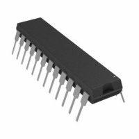
AD420AN-32 Analog Devices Inc, AD420AN-32 Datasheet - Page 9

AD420AN-32
Manufacturer Part Number
AD420AN-32
Description
IC DAC SRL 16BIT 24-DIP
Manufacturer
Analog Devices Inc
Datasheet
1.AD420ANZ-32.pdf
(16 pages)
Specifications of AD420AN-32
Data Interface
Serial
Settling Time
10µs
Rohs Status
RoHS non-compliant
Number Of Bits
16
Number Of Converters
1
Voltage Supply Source
Single Supply
Power Dissipation (max)
176mW
Operating Temperature
-40°C ~ 85°C
Mounting Type
Through Hole
Package / Case
24-DIP (0.300", 7.62mm)
Resolution (bits)
16bit
Digital Ic Case Style
DIP
No. Of Pins
24
Operating Temperature Range
-40°C To +85°C
Update Rate
0.0004MSPS
Lead Free Status / RoHS Status
Contains lead / RoHS non-compliant
Available stocks
Company
Part Number
Manufacturer
Quantity
Price
Company:
Part Number:
AD420AN-32
Manufacturer:
CONEXANT
Quantity:
30 000
Part Number:
AD420AN-32
Manufacturer:
ADI/亚德诺
Quantity:
20 000
THEORY OF OPERATION
The AD420 uses a sigma-delta (Σ-Δ) architecture to carry out
the digital-to-analog conversion. This architecture is particularly
well suited for the relatively low bandwidth requirements of the
industrial control environment because of its inherent
monotonicity at high resolution.
In the AD420 a second order modulator is used to keep com-
plexity and die size to a minimum. The single bit stream from
the modulator controls a switched current source that is then
filtered by two, continuous time resistor-capacitor sections.
The capacitors are the only external components that have to be
added for standard current-out operation. The filtered current
is amplified and mirrored to the supply rail so that the application
simply sees a 4 mA–20 mA, 0 mA–20 mA, or 0 mA–24 mA
current source output with respect to ground. The AD420
implementing low voltage digital logic with high performance
and high voltage analog circuitry.
The AD420 can also provide a voltage output instead of a current
loop output if desired. The addition of a single external amplifier
allows the user to obtain 0 V–5 V, 0 V–10 V, ±5 V, or ±10 V.
The AD420 has a loop fault detection circuit that warns if the
voltage at I
to an open-loop circuit or insufficient power supply voltage. The
FAULT DETECT is an active low open drain signal so that one
can connect several AD420s together to one pull-up resistor for
global error detection. The pull-up resistor can be tied to the
V
The I
internal amplifier as shown in the functional block diagram.
The internal circuitry that develops the fault output avoids
using a comparator with window limits since this would require
an actual output error before the FAULT DETECT output
becomes active. Instead, the signal is generated when the
internal amplifier in the output stage of the AD420 has less than
is manufactured on a BiCMOS process that is well suited to
LL
pin, or an external +5 V logic supply.
OUT
current is controlled by a PMOS transistor and an
OUT
attempts to rise above the compliance range, due
Rev. H | Page 9 of 16
approximately one volt remaining of drive capability (when
the gate of the output PMOS transistor nearly reaches ground).
Thus the FAULT DETECT output activates slightly before the
compliance limit is reached. Since the comparison is made
within the feedback loop of the output amplifier, the output
accuracy is maintained by its open-loop gain, and no output
error occurs before the fault detect output becomes active.
The 3-wire digital interface, comprising DATA IN, CLOCK,
and LATCH, interfaces to all commonly used serial micropro-
cessors without the addition of any external glue logic. Data is
loaded into an input register under control of CLOCK and is
loaded to the DAC when LATCH is strobed. If a user wants to
minimize the number of galvanic isolators in an intrinsically
safe application, the AD420 can be configured to run in
asynchronous mode. This mode is selected by connecting the
LATCH pin to V
must then be combined with a start and stop bit to frame the
information and trigger the internal LATCH signal.
DATA OUT
SELECT 1
SELECT 2
REF OUT
DATA IN
RANGE
RANGE
CLOCK
CLEAR
REF IN
LATCH
V
LL
14
15
10
2
6
7
8
9
5
4
REGISTER
DATA I/P
CC
Figure 5. Functional Block Diagram
through a current limiting resistor. The data
REFERENCE
OFFSET
CLOCK
16-BIT
TRIM
DAC
16
AD420
CAP 1 CAP 2
SWITCHED
FILTERING
CURRENT
SOURCES
20
4kΩ
AND
V
23
CC
21
GND
40Ω
11
1.25kΩ
19
18
17
3
AD420
BOOST
I
V
FAULT
DETECT
OUT
OUT


