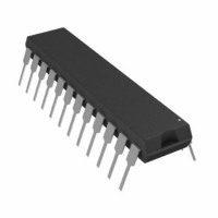
AD7245JN Analog Devices Inc, AD7245JN Datasheet - Page 11

AD7245JN
Manufacturer Part Number
AD7245JN
Description
IC DAC 12BIT W/REF 24-DIP
Manufacturer
Analog Devices Inc
Series
DACPORT®r
Datasheet
1.AD7245AARZ.pdf
(16 pages)
Specifications of AD7245JN
Mounting Type
Through Hole
Rohs Status
RoHS non-compliant
Settling Time
7µs
Number Of Bits
12
Data Interface
Parallel
Number Of Converters
1
Voltage Supply Source
Dual ±
Power Dissipation (max)
210mW
Operating Temperature
-40°C ~ 85°C
Package / Case
24-DIP (0.300", 7.62mm)
Resolution (bits)
12bit
No. Of Pins
24
Peak Reflow Compatible (260 C)
No
Update Rate
0.143MSPS
No. Of Bits
12 Bit
Leaded Process Compatible
No
Interface Type
Parallel
Lead Free Status / RoHS Status
Contains lead / RoHS non-compliant
Available stocks
Company
Part Number
Manufacturer
Quantity
Price
Part Number:
AD7245JN
Manufacturer:
ADI/亚德诺
Quantity:
20 000
UNIPOLAR (0 V TO 5 V) CONFIGURATION
The 0 V to 5 V output voltage range is achieved by tying R
R
AD7248A can be operated single supply (V
ply. The table for output voltage versus digital code is as in Table
III, with 2 × V
BIPOLAR CONFIGURATION
The bipolar configuration for the AD7245A/AD7248A, which
gives an output voltage range from –5 V to +5 V, is achieved by
connecting the R
and V
dual supplies to achieve this output voltage range. The code
table for bipolar operation is shown in Table IV.
DAC Latch Contents
MSB
1 1 1 1
1 0 0 0
1 0 0 0
0 1 1 1
0 0 0 0
0 0 0 0
NOTE: 1 LSB = 2 × V
AGND BIAS
The AD7245A/AD7248A AGND pin can be biased above sys-
tem GND (AD7245A/AD7248A DGND) to provide an offset
“zero” analog output voltage level. With unity gain on the
amplifier (R
expressed as:
where D is a fractional representation of the digital word in the
DAC latch and V
AD7248A AGND pin.
Because the current flowing out of the AGND pin varies with
digital code, the AGND pin should be driven from a low imped-
ance source. A circuit configuration is outlined for AGND bias
in Figure 9 using the AD589, a +1.23 V bandgap reference.
If a gain of 2 is used on the buffer amplifier the output voltage,
V
FB
OUT
and V
is expressed as
OUT
1 LSB = V
. The AD7245A/AD7248A must be operated from
OUT
1 1 1 1
0 0 0 0
0 0 0 0
1 1 1 1
0 0 0 0
0 0 0 0
OFS
REF
together. For this output range the AD7245A/
= V
Table IV. Bipolar Code Table
OFS
V
BIAS
replaced by V
V
OUT
REF
OUT
OUT
input to REF OUT and connecting R
is the voltage applied to the AD7245A/
(2
LSB
1 1 1 1
0 0 0 1
0 0 0 0
1 1 1 1
0 0 0 1
0 0 0 0
= 2(V
REF
= R
–12
= V
) = V
(2
FB
BIAS
BIAS
–11
) the output voltage, V
) = V
REF
REF
+ D
Analog Output, V
+V
+V
–V
–V
–V
+ D
. Note that for this range
REF
REF
REF
REF
REF
REF
0 V
×
×
×
V
×
×
4096
V
SS
REF
1
REF
2048
= 0 V) or dual sup-
2048
2047
2048
2048
2048
2047
2048
2048
1
1
)
1
.
= –V
OUT
OUT
REF
OFS
is
FB
,
In this case care must be taken to ensure that the maximum
output voltage is not greater than V
overhead must be greater than 3 V to ensure correct operation
of the part. Note that V
must be referenced to DGND (system GND). The entire circuit
can be operated in single supply with the V
AD7245A/AD7248A connected to system GND.
V
PROGRAMMABLE CURRENT SINK
Figure 10 shows how the AD7245A/AD7248A can be config-
ured with a power MOSFET transistor, the VN0300M, to
provide a programmable current sink from V
The VN0300M is placed in the feedback of the AD7245A/
AD7248A amplifier. The entire circuit can be operated in single
supply by tying the V
The sink current, I
0.1 F
Using the VN0300M, the voltage drop across the load can typi-
cally be as large as V
5 V. Therefore, for a current of 50 mA flowing in the R1 (with
all 1s in the DAC register) the maximum load is 200 Ω with
V
up to 500 mA and still function correctly in the circuit, but in
practice the circuit must be used with larger values of V
otherwise it requires a very small load.
BIAS
SOURCE
27k
DIGITAL CIRCUITRY
OMITTED FOR CLARITY.
+
–
DIGITAL CIRCUITRY
OMITTED FOR CLARITY.
15V
0.1 F
AD589
AGND
= 15 V. The VN0300M can actually handle currents
+
REF
REF OUT
10 F
10
+
V
SINK
REF
REF
REF OUT
10 F
SS
SOURCE
10
, can be expressed as:
I
DD
of the AD7245A/AD7248A to AGND.
SINK
DGND
V
REF
DAC
and V
R
=
OFS
–6 V) with V
2R
AD7245A/AD7248A
AD7245A/AD7248A
DGND
D ×V
AGND
SS
DAC
R1
for the AD7245A/AD7248A
R
OFS
2R
AD7245A/AD7248A
REF
DD
V
DD
2R
–3 V. The V
OUT
SS
V
SS
V
pin of the
DD
DD
of the DAC at
2R
R
V
OUT
or V
FB
V
SS
DD
V
SOURCE
SOURCE
SOURCE
–V
R
V
FB
OUT
LOAD
VN0300M
OUT
R1
SYSTEM
I
SINK
GND
.


