AD7243BN Analog Devices Inc, AD7243BN Datasheet - Page 6
AD7243BN
Manufacturer Part Number
AD7243BN
Description
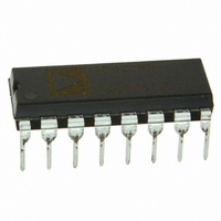
IC DAC 12BIT W/AMP W/REF 16-DIP
Manufacturer
Analog Devices Inc
Series
DACPORT®r
Datasheet
1.AD7243ANZ.pdf
(12 pages)
Specifications of AD7243BN
Rohs Status
RoHS non-compliant
Settling Time
10µs
Number Of Bits
12
Data Interface
Serial
Number Of Converters
1
Voltage Supply Source
Dual ±
Power Dissipation (max)
100mW
Operating Temperature
-40°C ~ 85°C
Mounting Type
Through Hole
Package / Case
16-DIP (0.300", 7.62mm)
Available stocks
Company
Part Number
Manufacturer
Quantity
Price


AD7243
0 V, to allow full sink capability of 2.5 mA over the entire
output range and to eliminate the effects of negative offsets on
the transfer characteristic (outlined previously). A plot of the
output sink capability of the amplifier is shown in Figure 5.
DIGITAL INTERFACE
The AD7243 contains an input serial to parallel shift register
and a DAC latch. A simplified diagram of the input loading
SCLK
SYNC
LDAC
SDIN
CLR
3
2
0
*
1
= DON'T CARE
0
V
DCEN
SYNC
LDAC
SCLK
SDIN
SS
CLR
= –15V
2
OUTPUT VOLTAGE – Volts
4
t
2
DB15
V
SS
= 0V
*
RESET
6
DB14
COUNTER/
DECODER
÷
*
16
AUTO – UPDATE
CIRCUITRY
8
EN
DB13
t
1
*
10
GATING
SIGNAL
DB12
*
GATED
SCLK
circuitry is shown in Figure 6. Serial data on the SDIN input is
loaded to the input register under control of DCEN, SYNC and
SCLK. When a complete word is held in the shift register, it
may then be loaded into the DAC latch under control of
LDAC. Only the data in the DAC latch determines the analog
output on the AD7243.
The DCEN (daisy-chain enable) input is used to select either a
standalone mode or a daisy-chain mode. The loading format is
slightly different depending on which mode is selected.
Serial Data Loading Format (Standalone Mode)
With DCEN at Logic 0 the standalone mode is selected. In this
mode a low SYNC input provides the frame synchronization
signal which tells the AD7243 that valid serial data on the SDIN
input will be available for the next 16 falling edges of SCLK. An
internal counter/decoder circuit provides a low gating signal so
that only 16 data bits are clocked into the input shift register.
After 16 SCLK pulses the internal gating signal goes inactive
(high) thus locking out any further clock pulses. Therefore, ei-
ther a continuous clock or a burst clock source may be used to
clock in the data.
The SYNC input should be taken high after the complete 16-bit
word is loaded in.
t
4
DB11
MSB
t
5
INPUT SHIFT REGISTER (16 BITS)
DAC LATCH (12 BITS)
DB0
LSB
t
3
t
6
t
7
SDO
t
8
t
9
Related parts for AD7243BN
Image
Part Number
Description
Manufacturer
Datasheet
Request
R

Part Number:
Description:
±1.7g Dual-Axis IMEMS Accelerometer Evaluation Board
Manufacturer:
Analog Devices Inc
Datasheet:

Part Number:
Description:
Inertial Sensor Evaluation System
Manufacturer:
Analog Devices Inc
Datasheet:
Part Number:
Description:
Manufacturer:
Analog Devices Inc
Datasheet:
Part Number:
Description:
Manufacturer:
Analog Devices Inc
Datasheet:
Part Number:
Description:
Manufacturer:
Analog Devices Inc
Datasheet:
Part Number:
Description:
Manufacturer:
Analog Devices Inc
Datasheet:
Part Number:
Description:
Manufacturer:
Analog Devices Inc
Datasheet:
Part Number:
Description:
Manufacturer:
Analog Devices Inc
Datasheet:
Part Number:
Description:
Manufacturer:
Analog Devices Inc
Datasheet:
Part Number:
Description:
Manufacturer:
Analog Devices Inc
Datasheet:
Part Number:
Description:
Manufacturer:
Analog Devices Inc
Datasheet:
Part Number:
Description:
Manufacturer:
Analog Devices Inc
Datasheet:
Part Number:
Description:
Manufacturer:
Analog Devices Inc
Datasheet: