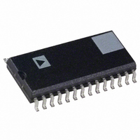
DAC8408FSZ Analog Devices Inc, DAC8408FSZ Datasheet - Page 9

DAC8408FSZ
Manufacturer Part Number
DAC8408FSZ
Description
IC DAC 8BIT QUAD W/MEMORY 28SOIC
Manufacturer
Analog Devices Inc
Datasheet
1.DAC8408FSZ-REEL.pdf
(16 pages)
Specifications of DAC8408FSZ
Data Interface
Parallel
Settling Time
190ns
Number Of Bits
8
Number Of Converters
4
Voltage Supply Source
Single Supply
Operating Temperature
-40°C ~ 85°C
Mounting Type
Surface Mount
Package / Case
28-SOIC (7.5mm Width)
Resolution (bits)
8bit
Input Channel Type
Parallel
Supply Voltage Range - Analogue
4.5V To 5.5V
Supply Current
50µA
Digital Ic Case Style
SOIC
No. Of
RoHS Compliant
Number Of Channels
4
Resolution
8b
Interface Type
Parallel
Single Supply Voltage (typ)
5V
Dual Supply Voltage (typ)
Not RequiredV
Architecture
R-2R
Power Supply Requirement
Single
Output Type
Current
Single Supply Voltage (min)
4.5V
Single Supply Voltage (max)
5.5V
Dual Supply Voltage (min)
Not RequiredV
Dual Supply Voltage (max)
Not RequiredV
Operating Temp Range
-40C to 85C
Operating Temperature Classification
Industrial
Mounting
Surface Mount
Pin Count
28
Lead Free Status / RoHS Status
Lead free / RoHS Compliant
Power Dissipation (max)
-
Lead Free Status / Rohs Status
Compliant
Available stocks
Company
Part Number
Manufacturer
Quantity
Price
Part Number:
DAC8408FSZ
Manufacturer:
ADI/亚德诺
Quantity:
20 000
DIGITAL SECTION
Figure 5 shows the digital input/output structure for one bit.
The digital WR, WR, and RD controls shown in the figure are
internally generated from the external A/B, R/W, DS1, and DS2
signals. The combination of these signals decide which DAC is
selected. The digital inputs are CMOS inverters, designed such
that TTL input levels (2.4 V and 0.8 V) are converted into
CMOS logic levels. When the digital input is in the region of 1.2 V
to 1.8 V, the input stages operate in their linear region and draw
current from the +5 V supply (see Typical Supply Current vs.
Logic Level curve on page 6). It is recommended that the digital
input voltages be as close to V
order to minimize supply currents. This allows maximum sav-
ings in power dissipation inherent with CMOS devices. The
three-state readback digital output drivers (in the active mode)
provide TTL-compatible digital outputs with a fan-out of one
TTL load. The three state digital readback leakage-current is
typically 5 nA.
REV. A
Figure 4. Equivalent DAC Circuit (AII Digital Inputs LOW)
Figure 5. Digital Input/Output Structure
DD
and DGND as is practical in
–9–
INTERFACE LOGIC SECTION
DAC Operating Modes
• All DACs in HOLD MODE.
• DAC A, B, C, or D individually selected (WRITE MODE).
• DAC A, B, C, or D individually selected (READ MODE).
• DACs A and C simultaneously selected (WRITE MODE).
• DACs B and D simultaneously selected (WRITE MODE).
DAC Selection: Control inputs, DS1, DS2, and A/B select
which DAC can accept data from the input port (see Mode Se-
lection Table).
Mode Selection: Control inputs DS and R/W control the oper-
ating mode of the selected DAC.
Write Mode: When the control inputs DS and R/W are both
low, the selected DAC is in the write mode. The input data
latches of the selected DAC are transparent, and its analog out-
put responds to activity on the data inputs DB0–DB7.
Hold Mode: The selected DAC latch retains the data that was
present on the bus line just prior to DS or R/W going to a high
state. All analog outputs remain at the values corresponding to
the data in their respective latches.
Read Mode: When DS is low and R/W is high, the selected
DAC is in the read mode, and the data held in the appropriate
latch is put back onto the data bus.
DS1
L
L
H
H
L
L
H
H
L
L
H
L
L
L = Low State, H = High State, X = Irrelevant
Control Logic
DS2 A/B
H
H
L
L
H
H
L
L
L
L
H
L
L
H
L
H
L
H
L
H
L
H
L
X
H
L
MODE SELECTION TABLE
R/W
L
L
L
L
H
H
H
H
L
L
X
H
H
Mode
WRITE
WRITE
WRITE
WRITE
READ
READ
READ
READ
WRITE
WRITE
HOLD
HOLD
HOLD
DAC8408
DAC
A
B
C
D
A
B
C
D
A&C
B&D
A/B/C/D
A/B/C/D
A/B/C/D


