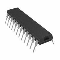
AD7245AAN Analog Devices Inc, AD7245AAN Datasheet - Page 6

AD7245AAN
Manufacturer Part Number
AD7245AAN
Description
IC DAC 12BIT LC2MOS 24-DIP
Manufacturer
Analog Devices Inc
Series
DACPORT®r
Datasheet
1.AD7245AARZ.pdf
(16 pages)
Specifications of AD7245AAN
Mounting Type
Through Hole
Rohs Status
RoHS non-compliant
Settling Time
7µs
Number Of Bits
12
Data Interface
Parallel
Number Of Converters
1
Voltage Supply Source
Dual ±
Power Dissipation (max)
210mW
Operating Temperature
-40°C ~ 85°C
Package / Case
24-DIP (0.300", 7.62mm)
Resolution (bits)
12bit
No. Of Pins
24
Update Rate
0.143MSPS
Peak Reflow Compatible (260 C)
No
No. Of Bits
12 Bit
Leaded Process Compatible
No
Interface Type
Serial
Lead Free Status / RoHS Status
Contains lead / RoHS non-compliant
Available stocks
Company
Part Number
Manufacturer
Quantity
Price
Part Number:
AD7245AAN
Manufacturer:
ADI/亚德诺
Quantity:
20 000
AD7245A/AD7248A
Pin
10
11
12
13
2
3
4
5
6
7
8
9
l
(MSB) DB7
REF OUT
Mnemonic
V
R
REF OUT
AGND
DB7
DB6
DB5
DB4
DB3
DGND
DB2
DB1
DB0
AGND
DGND
SS
OFS
R
DB6
DB5
DB4
DB3
V
OFS
SS
10
1
2
3
4
5
6
7
8
9
DIP and SOIC
(NOT TO SCALE)
AD7248A
TOP VIEW
supply operation).
access to the on-chip application resistors
and allows different output voltage ranges.
is provided at this pin and is used when
configuring the part for bipolar outputs.
Description
Negative Supply Voltage (0 V for single
Bipolar Offset Resistor. This provides
Reference Output. The on-chip reference
Analog Ground.
Data Bit 7.
Data Bit 6.
Data Bit 5.
Data Bit 4.
Data Bit 3.
Digital Ground.
Data Bit 2/Data Bit 10.
Data Bit 1/Data Bit 9.
Data Bit 0 (LSB)/Data Bit 8.
20
19
18
17
16
15
14
13
12
11
CSMSB
V
R
V
LDAC
WR
CSLSB
DB0 (LSB)
DB1
DB2
OUT
DD
FB
AD7248A PIN FUNCTION DESCRIPTIONS
AD7248A PIN CONFIGURATIONS
(MSB) DB7
AGND
DB6
DB5
DB4
(ANY PACKAGE)
4
5
6
7
8
3
(NOT TO SCALE)
9
PLCC
AD7248A
TOP VIEW
10
2
11
1
PIN 1
IDENTIFIER
Pin
14
15
16
17
18
19
20
20
12
19
13
Mnemonic
CSMSB
CSLSB
WR
LDAC
V
R
V
18
17
16
15
14
DD
FB
OUT
LDAC
WR
CSLSB
CSMSB
V
DD
Description
Chip Select Input for MS Nibble. (Active
LOW). This selects the upper 4 bits of the
input latch. Input data is right justified.
Chip Select Input for LS byte. (Active
LOW). This selects the lower 8 bits of the
input latch.
Write Input. This is used in conjunction
with CSMSB and CSLSB to load data
into the input latch of the AD7248A.
Load DAC Input (Active LOW). This is
an asynchronous input which when active
transfers data from the input latch to the
DAC latch.
Positive Supply Voltage.
Feedback Resistor. This allows access to
the amplifier’s feedback loop.
Output Voltage. Three different output
voltage ranges can be chosen: 0 V to 5 V,
0 V to 10 V or –5 V to +5 V.
(MSB) DB7
AGND
DB6
DB5
DB4
4
5
6
7
8
(NOT TO SCALE)
9
3
LCCC
AD7248A
TOP VIEW
10 11 12 13
2
1
20 19
18
17
16
15
14
V
LDAC
WR
CSLSB
CSMSB
DD


