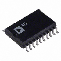
AD7849AR-REEL Analog Devices Inc, AD7849AR-REEL Datasheet - Page 5

AD7849AR-REEL
Manufacturer Part Number
AD7849AR-REEL
Description
IC DAC 16BIT SRL INP 20-SOIC
Manufacturer
Analog Devices Inc
Datasheet
1.AD7849BRZ.pdf
(20 pages)
Specifications of AD7849AR-REEL
Rohs Status
RoHS non-compliant
Settling Time
7µs
Number Of Bits
16
Data Interface
Serial
Number Of Converters
1
Voltage Supply Source
Analog and Digital, Dual ±
Power Dissipation (max)
100mW
Operating Temperature
-40°C ~ 85°C
Mounting Type
Surface Mount
Package / Case
20-SOIC (7.5mm Width)
AC PERFORMANCE CHARACTERISTICS
These characteristics are included for design guidance and are no subject to test. V
−15.75 V; V
Table 3.
Parameter
DYNAMIC PERFORMANCE
1
TIMING CHARACTERISTICS
V
unless otherwise noted. Guaranteed by characterization. All input signals are specified tr = tf = 5 ns (10% to 90% of 5 V and timed from a
voltage level of 1.6 V.
Table 4.
Parameter
t
t
t
t
t
t
t
t
t
1
2
1
2
3
4
5
6
7
r
f
LDAC = 0. Settling time does not include deglitching time of 5 μs (typical).
SCLK mark/space ratio range is 40/60 to 60/40.
SDO load capacitance is 50 pF.
1
2
DD
Output Settling Time
Slew Rate
Digital-to-Analog Glitch Impulse
AC Feedthrough
Digital Feedthrough
Output Noise Voltage Density, 1 kHz to 100 kHz
= 14.25 V to 15.75 V; V
CC
= 4.75 V to 5.25 V; R
Limit at 25°C (All Versions)
200
50
70
10
40
80
80
30
30
1
SS
= −14.25 V to −15.75 V; V
OFS
connected to 0 V.
Limit at T
200
50
70
10
40
80
80
30
30
A, B, C Versions
7
10
250
150
1
5
80
4
CC
= 4.75 V to 5.25 V; R
Rev. C | Page 5 of 20
MIN
, T
MAX
(All Versions)
nV-sec typ
Unit
μs typ
μs typ
V/μs typ
nV-sec typ
nV-sec typ
mV p-p typ
nV/√Hz typ
L
= 2 kΩ, C
REF+
= 5 V; V
Test Conditions/Comments
To 0.006% FSR. V
To 0.003% FSR. V
DAC alternatively loaded with 00 … 00 and
111 … 11. V
BIN/COMP set to 1. V
LDAC frequency = 100 kHz.
V
DAC loaded with all 0s. BIN/COMP set to 0.
DAC alternatively loaded with all 1s and 0s.
SYNC high.
Measured at V
BIN/COMP set to 0.
REF−
L
= 200 pF. All specifications T
Unit
ns min
ns min
ns min
ns min
ns min
ns max
ns min
μs max
μs max
= 0 V, V
DD
= 14.25 V to 15.75 V; V
OUT
REF+
OUT
loaded. LDAC permanently low.
Test Conditions/Comments
SCLK cycle time
SYNC-to-SCLK setup time
SYNC-to-SCLK hold time
Data setup time
Data hold time
SCLK falling edge to SDO valid
LDAC, CLR pulse width
Digital input rise time
Digital input fall time
= 1 V rms, 10 kHz sine wave.
OUT
OUT
. V
REF+
loaded. V
loaded. V
REF−
= V
= −5 V.
REF−
REF−
REF−
= 0 V.
SS
= 0 V.
= −5 V.
MIN
= −14.25 V to
to T
AD7849
MAX
,


