AD558JN Analog Devices Inc, AD558JN Datasheet - Page 6
AD558JN
Manufacturer Part Number
AD558JN
Description
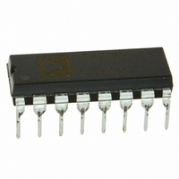
IC DAC 8BIT V-OUT 16-DIP
Manufacturer
Analog Devices Inc
Series
DACPORT®r
Datasheet
1.AD558JNZ.pdf
(8 pages)
Specifications of AD558JN
Data Interface
Parallel
Settling Time
800ns
Rohs Status
RoHS non-compliant
Number Of Bits
8
Number Of Converters
1
Voltage Supply Source
Single Supply
Power Dissipation (max)
375mW
Operating Temperature
0°C ~ 70°C
Mounting Type
Through Hole
Package / Case
16-DIP (0.300", 7.62mm)
Resolution (bits)
8bit
Digital Ic Case Style
DIP
No. Of Pins
16
Operating Temperature Range
0°C To +70°C
Update Rate
1.25MSPS
Lead Free Status / RoHS Status
Contains lead / RoHS non-compliant
Available stocks
Company
Part Number
Manufacturer
Quantity
Price

Part Number:
AD558JN
Manufacturer:
ADI/亚德诺
Quantity:
20 000
Company:
Part Number:
AD558JN/+
Manufacturer:
AMI
Quantity:
6 236
Company:
Part Number:
AD558JNZ
Manufacturer:
AD
Quantity:
2 255
Part Number:
AD558JNZ
Manufacturer:
ADI/亚德诺
Quantity:
20 000


AD558
USE OF V
Separate access to the feedback resistor of the output amplifier
allows additional application versatility. Figure 8a shows how
I
putting the drops “inside the loop.” Figure 8b shows how the
separate sense may be used to provide a higher output current
by feeding back around a simple current booster.
OPTIMIZING SETTLING TIME
In order to provide single-supply operation and zero-based
output voltage ranges, the AD558 output stage has a passive
“pull-down” to ground. As a result, settling time for negative
going output steps may be longer than for positive-going output
steps. The relative difference depends on load resistance and
capacitance. If a negative power supply is available, the
negative-going settling time may be improved by adding a pull-
down resistor from the output to the negative supply as shown
in Figure 9. The value of the resistor should be such that, at
zero voltage out, current through that resistor is 0.5 mA max.
BIPOLAR OUTPUT RANGES
The AD558 was designed for operation from a single power
supply and is thus capable of providing only unipolar (0 V to
+2.56 V and 0 V to 10 V) output ranges. If a negative supply is
R drops in long lines to remote loads may be cancelled by
a. Compensation for I
12
12
OUT
DATA
INPUTS
CS OR CE
DAC
V OUTPUT
t
t
t
t
W
DH
DS
SETTLING
AD558
AD558
13
13
= STORAGE PULSE WIDTH = 200ns MIN
SENSE
= DATA SETUP TIME = 200ns MIN
= DATA HOLD TIME = 10ns MIN
GND
GND
Figure 8. Use of V
b. Output Current Booster
0.8V
0.8V
Figure 7. AD558 Timing
14
14
= DAC OUTPUT SETTLING TIME TO 1/2 LSB
GAIN
SELECT
GAIN
SELECT
16
15
16
15
V
V
V
V
OUT
OUT
OUT
OUT
t
R Drops in Output Lines
W
t
t
SETTLING
DS
SENSE
SENSE
OUT
Sense
V
CC
2N2222
t
R
DH
L
R
1/2 LSB
L
0V TO +2.56V
2.0V
2.0V
0V TO +10V
V
OUT
V
OUT
–6–
available, bipolar output ranges may be achieved by suitable
output offsetting and scaling. Figure 10 shows how a 1.28 volt
output range may be achieved when a –5 volt power supply is
available. The offset is provided by the AD589 precision 1.2 volt
reference which will operate from a +5 volt supply. The AD544
output amplifier can provide the necessary 1.28 volt output
swing from 5 volt supplies. Coding is complementary offset
binary.
MEASURING OFFSET ERROR
One of the most commonly specified endpoint errors associated
with real-world nonideal DACs is offset error.
In most DAC testing, the offset error is measured by applying
the zero-scale code and measuring the output deviation from 0
volts. There are some DACs, like the AD558 where offset errors
may be present but not observable at the zero scale, because of
other circuit limitations (such as zero coinciding with single-
supply ground) so that a nonzero output at zero code cannot be
read as the offset error. Factors like this make testing the
AD558 a little more complicated.
By adding a pulldown resistor from the output to a negative
supply as shown in Figure 11, we can now read offset errors
at zero code that may not have been observable due to circuit
limitations. The value of the resistor should be such that, at zero
voltage out, current through the resistor is 0.5 mA max.
Figure 10. Bipolar Operation of AD558 from 5 V Supplies
12
AD558
Figure 9. Improved Settling Time
AD558
13
a. 0 V to 2.56 V Output Range
AD589
0.01 F
OUTPUT
16
14
AMP
15
–5V
V
4.7k
V
–1.2V
OUT
16
15
IN
16
15
14
13
= 0V TO +2.56V
BIPOLAR
ADJUST
OFFSET
V
V
4.53k
OUT
OUT
V
V
500
5k
OUT
OUT
AGND
NEGATIVE
SUPPLY
SENSE
V
SENSE
SELECT
OUT
INPUT CODE
–V
1.5k
00000000
10000000
11111111
R
AD544
V
P-D
0.5mA
EE
+5V
–5V
= 2x V
R
0.01 F
0.01 F
L
5k
(in k )
EE
V
+128V
0V
–1.27V
V
+1.28 TO
–1.27
OUT
REV. A
O
Related parts for AD558JN
Image
Part Number
Description
Manufacturer
Datasheet
Request
R

Part Number:
Description:
±1.7g Dual-Axis IMEMS Accelerometer Evaluation Board
Manufacturer:
Analog Devices Inc
Datasheet:

Part Number:
Description:
Inertial Sensor Evaluation System
Manufacturer:
Analog Devices Inc
Datasheet:
Part Number:
Description:
Manufacturer:
Analog Devices Inc
Datasheet:
Part Number:
Description:
Manufacturer:
Analog Devices Inc
Datasheet:
Part Number:
Description:
Manufacturer:
Analog Devices Inc
Datasheet:
Part Number:
Description:
Manufacturer:
Analog Devices Inc
Datasheet:
Part Number:
Description:
Manufacturer:
Analog Devices Inc
Datasheet:
Part Number:
Description:
Manufacturer:
Analog Devices Inc
Datasheet:
Part Number:
Description:
Manufacturer:
Analog Devices Inc
Datasheet:
Part Number:
Description:
Manufacturer:
Analog Devices Inc
Datasheet:
Part Number:
Description:
Manufacturer:
Analog Devices Inc
Datasheet:
Part Number:
Description:
Manufacturer:
Analog Devices Inc
Datasheet:
Part Number:
Description:
Manufacturer:
Analog Devices Inc
Datasheet: