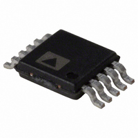
AD5663RBRMZ-3 Analog Devices Inc, AD5663RBRMZ-3 Datasheet - Page 6

AD5663RBRMZ-3
Manufacturer Part Number
AD5663RBRMZ-3
Description
IC DAC NANO 16BIT 1.25V 10-MSOP
Manufacturer
Analog Devices Inc
Series
nanoDAC™r
Specifications of AD5663RBRMZ-3
Data Interface
Serial
Settling Time
4µs
Number Of Bits
16
Number Of Converters
2
Voltage Supply Source
Single Supply
Power Dissipation (max)
5mW
Operating Temperature
-40°C ~ 105°C
Mounting Type
Surface Mount
Package / Case
10-MSOP, Micro10™, 10-uMAX, 10-uSOP
Resolution (bits)
16bit
Sampling Rate
220kSPS
Input Channel Type
Serial
Supply Voltage Range - Analog
2.7V To 3.6V, 4.5V To 5.5V
Supply Current
800µA
Lead Free Status / RoHS Status
Lead free / RoHS Compliant
For Use With
EVAL-AD5663REBZ - BOARD EVAL FOR AD5663
Lead Free Status / RoHS Status
Lead free / RoHS Compliant, Lead free / RoHS Compliant
Available stocks
Company
Part Number
Manufacturer
Quantity
Price
Part Number:
AD5663RBRMZ-3
Manufacturer:
ADI/亚德诺
Quantity:
20 000
Parameter
Output Voltage Settling Time
Slew Rate
Digital-to-Analog Glitch Impulse
Digital Feedthrough
Reference Feedthrough
Digital Crosstalk
Analog Crosstalk
DAC-to-DAC Crosstalk
Multiplying Bandwidth
Total Harmonic Distortion
Output Noise Spectral Density
Output Noise
AD5623R/AD5643R/AD5663R
Parameter
LOGIC INPUTS
POWER REQUIREMENTS
1
2
3
4
5
AC CHARACTERISTICS
V
Table 4.
1
2
3
Temperature range: B grade = −40°C to +105°C.
Linearity calculated using a reduced code range: AD5663R (Code 512 to Code 65,024), AD5643R (Code 128 to Code 16,256), and AD5623R (Code 32 to Code 4064).
Output unloaded.
Guaranteed by design and characterization, not production tested.
Interface inactive. All DACs active. DAC outputs unloaded.
Both DACs powered down.
Guaranteed by design and characterization, not production tested.
See the Terminology section.
Temperature range: B grade = −40°C to +105°C, typical at +25°C.
AD5623R
AD5643R
AD5663R
DD
Input Current
V
V
Pin Capacitance
V
INL
INH
DD
= 2.7 V to 5.5 V; R
I
V
V
I
V
DD
DD
, Input Low Voltage
, Input High Voltage
DD
DD
DD
(Normal Mode)
(All Power-Down Modes)
= 2.7 V to 3.6 V
= 2.7 V to 3.6 V
= 2.7 V to 3.6 V
1, 2
3
L
4
= 2 kΩ to GND; C
5
Min
L
= 200 pF to GND; V
Min
2
2.7
Typ
3
3.5
4
1.8
10
0.1
−90
0.1
1
4
1
4
340
−80
120
100
15
B Grade
Typ
3
19
200
800
0.2
4.5
5
7
Max
Rev. D | Page 6 of 32
1
REFIN
Max
±2
0.8
3.6
425
900
1
= V
Unit
μs
μs
μs
V/μs
nV-s
nV-s
dB
nV-s
nV-s
nV-s
nV-s
nV-s
kHz
dB
nV/√Hz
nV/√Hz
μV p-p
DD
; all specifications T
Unit
μA
V
V
pF
pF
V
μA
μA
μA
¼ to ¾ scale settling to ±0.5 LSB
¼ to ¾ scale settling to ±0.5 LSB
¼ to ¾ scale settling to ±2 LSB
Conditions/Comments
1 LSB change around major carry
V
External reference
Internal reference
External reference
Internal reference
V
V
DAC code = midscale, 1 kHz
DAC code = midscale, 10 kHz
0.1 Hz to 10 Hz
REF
REF
REF
= 2 V ± 0.1 V p-p, frequency 10 Hz to 20 MHz
= 2 V ± 0.1 V p-p
= 2 V ± 0.1 V p-p, frequency = 10 kHz
Conditions/Comments
All digital inputs
V
V
DIN, SCLK, and SYNC
LDAC and CLR
V
Internal reference off
Internal reference on
V
DD
DD
IH
IH
MIN
= V
= V
= 3 V
= 3 V
to T
DD
DD
and V
and V
MAX
, unless otherwise noted.
IL
IL
= GND
= GND
3


