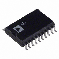
AD8802AR Analog Devices Inc, AD8802AR Datasheet - Page 8

AD8802AR
Manufacturer Part Number
AD8802AR
Description
IC DAC 8BIT 12CH W/SD 20-SOIC
Manufacturer
Analog Devices Inc
Series
TrimDAC®r
Datasheet
1.AD8804ARUZ-REEL.pdf
(16 pages)
Specifications of AD8802AR
Settling Time
600ns
Rohs Status
RoHS non-compliant
Number Of Bits
8
Data Interface
Serial
Number Of Converters
12
Voltage Supply Source
Single Supply
Power Dissipation (max)
60µW
Operating Temperature
-40°C ~ 85°C
Mounting Type
Surface Mount
Package / Case
20-SOIC (7.5mm Width)
Number Of Channels
12
Resolution
8b
Interface Type
Serial (3-Wire/SPI)
Single Supply Voltage (typ)
3/5V
Dual Supply Voltage (typ)
Not RequiredV
Architecture
R-2R
Power Supply Requirement
Single
Output Type
Voltage
Single Supply Voltage (min)
2.7V
Single Supply Voltage (max)
5.5V
Dual Supply Voltage (min)
Not RequiredV
Dual Supply Voltage (max)
Not RequiredV
Operating Temp Range
-40C to 85C
Operating Temperature Classification
Industrial
Mounting
Surface Mount
Pin Count
20
Lead Free Status / RoHS Status
Not Compliant
Available stocks
Company
Part Number
Manufacturer
Quantity
Price
Part Number:
AD8802ARU
Manufacturer:
ADI/亚德诺
Quantity:
20 000
Company:
Part Number:
AD8802ARU-REEL
Manufacturer:
AUDIENCE
Quantity:
37 338
Part Number:
AD8802ARUZ
Manufacturer:
ADI/亚德诺
Quantity:
20 000
APPLICATIONS
Supply Bypassing
Precision analog products, such as the AD8802/AD8804, re-
quire a well filtered power source. Since the AD8802/AD8804
operate from a single +3 V to +5 V supply, it seems convenient
to simply tap into the digital logic power supply. Unfortunately,
the logic supply is often a switch-mode design, which generates
noise in the 20 kHz to 1 MHz range. In addition, fast logic gates
can generate glitches hundred of millivolts in amplitude due to
wiring resistances and inductances.
If possible, the AD8802/AD8804 should be powered directly
from the system power supply. This arrangement, shown in Fig-
ure 20, will isolate the analog section from the logic switching
transients. Even if a separate power supply trace is not available,
however, generous supply bypassing will reduce supply-line in-
duced errors. Local supply bypassing consisting of a 10 F tan-
talum electrolytic in parallel with a 0.1 F ceramic capacitor is
recommended (Figure 21).
Figure 20. Use Separate Traces to Reduce Power Supply
Noise
AD8802/AD8804
The target DAC register is loaded with the last eight bits of the
serial data-word completing one DAC update. Twelve separate
12-bit data words must be clocked in to change all twelve out-
put settings.
All digital inputs are protected with a series input resistor and
parallel Zener ESD structure shown in Figure 19. Applies to
digital input pins CS, SDI, RS, SHDN, CLK
Digital inputs can be driven by voltages exceeding the AD8802/
AD8804 V
directly to the part when it is operated at 3 V.
Figure 19. Equivalent ESD Protection Circuit
DD
TTL/CMOS
CIRCUITS
Figure 18. Equivalent Control Logic
LOGIC
CLK
supply value. This allows 5 V logic to interface
POWER SUPPLY
SDI
CS
+5V
1k
+
TANT
10µF
REGISTER
DECODE
SERIAL
ADDR
LOGIC
0.1µF
DAC 1
DAC 2
DAC 12
. .
.
AD8802/
AD8804
–8–
Figure 21. Recommended Supply Bypassing for the
AD8802/AD8804
Buffering the AD8802/AD8804 Output
In many cases, the nominal 5 k output impedance of the
AD8802/AD8804 is sufficient to drive succeeding circuitry. If a
lower output impedance is required, an external amplifier can
be added. Several examples are shown in Figure 22. One ampli-
fier of an OP291 is used as a simple buffer to reduce the output
resistance of DAC A. The OP291 was chosen primarily for its
rail-to-rail input and output operation, but it also offers opera-
tion to less than 3 V, low offset voltage, and low supply current.
The next two DACs, B and C, are configured in a summing
arrangement where DAC C provides the coarse output voltage
setting and DAC B can be used for fine adjustment. The inser-
tion of R1 in series with DAC B attenuates its contribution to
the voltage sum node at the DAC C output.
Increasing Output Voltage Swing
An external amplifier can also be used to extend the output volt-
age swing beyond the power supply rails of the AD8802/AD8804.
This technique permits an easy digital interface for the DAC,
while expanding the output swing to take advantage of higher
voltage external power supplies. For example, DAC A of Fig-
ure 23 is configured to swing from –5 V to +5 V. The actual
output voltage is given by:
where D is the DAC input value (i.e., 0 to 255). This circuit can
be combined with the “fine/coarse” circuit of Figure 22 if, for
example, a very accurate adjustment around 0 V is desired.
V
Figure 22. Buffering the AD8802/AD8804 Output
REFL
V
REFH
AD8802/
AD8804
V
V
V
V
V
V
H
H
H
L
L
L
V
GND
+5V
V
DD
OUT
DIGITAL INTERFACING
OMITTED FOR CLARITY
+
10µF
1
R1
100k
R
R
F
S
0.1µF
256
OP291
D
AD8802/
AD8804
DGND
V
+5V
DD
5 V – 5 V
SIMPLE BUFFER
0V TO 5V
SUMMER CIRCUIT
WITH FINE TRIM
ADJUSTMENT
REV. 0


