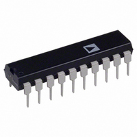
AD7945BNZ Analog Devices Inc, AD7945BNZ Datasheet - Page 5

AD7945BNZ
Manufacturer Part Number
AD7945BNZ
Description
IC DAC 12BIT MULT PARALL 20DIP
Manufacturer
Analog Devices Inc
Datasheet
1.AD7943BNZ.pdf
(16 pages)
Specifications of AD7945BNZ
Data Interface
Parallel
Settling Time
600ns
Number Of Bits
12
Number Of Converters
1
Voltage Supply Source
Single Supply
Power Dissipation (max)
25µW
Operating Temperature
-40°C ~ 85°C
Mounting Type
Through Hole
Package / Case
20-DIP (0.300", 7.62mm)
Resolution (bits)
12bit
Sampling Rate
1.7MSPS
Input Channel Type
Parallel
Supply Current
5µA
Digital Ic Case Style
DIP
No. Of Pins
20
Package
20PDIP N
Resolution
12 Bit
Conversion Rate
1.7 MSPS
Architecture
R-2R
Digital Interface Type
Parallel
Number Of Outputs Per Chip
1
Output Type
Current
Full Scale Error
±2 LSB
Integral Nonlinearity Error
±0.5 LSB
Maximum Settling Time
0.6(Typ) us
Lead Free Status / RoHS Status
Lead free / RoHS Compliant
Available stocks
Company
Part Number
Manufacturer
Quantity
Price
Part Number:
AD7945BNZ
Manufacturer:
ADI/亚德诺
Quantity:
20 000
REV. B
AD7943 TIMING SPECIFICATIONS
Parameter
t
t
t
t
t
t
t
t
NOTES
1
2
3
Specifications subject to change without notice.
STB
DS
DH
SRI
LD
CLR
ASB
SV
All input signals are specified with tr = tf = 5 ns (10% to 90% of 5 V) and timed from a voltage level of 1.6 V. tr and tf should not exceed 1 s on any digital input.
STB mark/space ratio range is 60/40 to 40/60.
t
SV
3
is measured with the load circuit of Figure 2 and defined as the time required for the output to cross 0.8 V or 2.4 V.
2
STB1,
STB2,
STB4
STB3
LD1,
LD2,
CLR
SRO
SRI
t
DB11(N)
DS
(MSB)
t
SRI
Limit @
V
60
15
35
55
55
55
0
60
t
DH
DD
t
STB
= +3 V to +3.6 V
DB10(N–1)
DB10(N)
t
SV
Figure 2. Load Circuit for Digital Output Timing Specifications
Limit @
V
40
10
25
35
35
35
0
35
DD
TO OUTPUT
Figure 1. AD7943 Timing Diagram
= +4.5 V to +5.5 V
1
PIN
(T
A
= T
50pF
MIN
C
L
to T
1.6mA
200 A
–5–
MAX
, unless otherwise noted)
I
I
OL
OH
Units
ns min
ns min
ns min
ns min
ns min
ns min
ns min
ns max
+2.1V
Description
Min Time Between Strobing Input Shift
Register and Loading DAC Register
STB Pulsewidth
Data Setup Time
Data Hold Time
SRI Data Pulsewidth
Load Pulsewidth
CLR Pulsewidth
STB Clocking Edge to SRO Data Valid Delay
AD7943/AD7945/AD7948
DB0(N)
DB0(N–1)
t
ASB
t
LD ,
t
CLR


