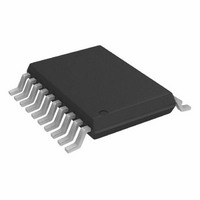
AD7801BRU Analog Devices Inc, AD7801BRU Datasheet - Page 13

AD7801BRU
Manufacturer Part Number
AD7801BRU
Description
IC DAC 8BIT PARALLEL INP 20TSSOP
Manufacturer
Analog Devices Inc
Datasheet
1.AD7801BRUZ-REEL.pdf
(16 pages)
Specifications of AD7801BRU
Rohs Status
RoHS non-compliant
Settling Time
1.2µs
Number Of Bits
8
Data Interface
Parallel
Number Of Converters
1
Voltage Supply Source
Single Supply
Power Dissipation (max)
12.9mW
Operating Temperature
-40°C ~ 105°C
Mounting Type
Surface Mount
Package / Case
20-TSSOP
Available stocks
Company
Part Number
Manufacturer
Quantity
Price
Part Number:
AD7801BRU
Manufacturer:
AD
Quantity:
20 000
Part Number:
AD7801BRUZ
Manufacturer:
ADI/亚德诺
Quantity:
20 000
Part Number:
AD7801BRUZ#
Manufacturer:
ADI/亚德诺
Quantity:
20 000
Part Number:
AD7801BRUZ-REEL
Manufacturer:
ADI/亚德诺
Quantity:
20 000
Part Number:
AD7801BRUZ-REEL7
Manufacturer:
ADI/亚德诺
Quantity:
20 000
Power Supply Bypassing and Grounding
In any circuit where accuracy is important, careful consideration
of the power supply and ground return layout helps to ensure
the rated performance. The printed circuit board on which the
AD7801 is mounted should be designed so that the analog and
digital sections are separated and confined to certain areas of the
board. If the AD7801 is in a system where multiple devices
require an AGND to DGND connection, the connection should
be made at one point only, a star ground point which should be
established as closely as possible to the AD7801. The AD7801
should have ample supply bypassing of 10 F in parallel with
0.1 F located as close to the package as possible, ideally right
up against the device. The 10 F capacitors are the tantalum
bead type. The 0.1 F capacitors should have low Effective
Series Resistance (ESR) and Effective Series Inductance (ESI),
such as the common ceramic types, which provide a low
impedance path to ground at high frequencies to handle
transient currents due to internal logic switching.
REV. 0
–13–
The power supply lines of the AD7801 should use as large a
trace as possible to provide low impedance paths and reduce the
effects of glitches on the supply line. Fast switching signals like
clocks should be shielded with digital ground to avoid radiating
noise to other parts of the board and should never be run near
reference inputs. Avoid crossover of digital and analog signals.
Traces on opposite sides of the board should run at right angles
to each other. This reduces the effect of feedthrough through
the board. A microstrip technique is by far the best, but not
always possible with a double-sided board. In this technique, the
component side of the board is dedicated to the ground plane
while signal traces are placed on the solder side.
AD7801


