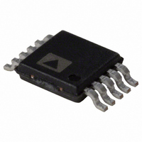
AD5304ARMZ Analog Devices Inc, AD5304ARMZ Datasheet - Page 17

AD5304ARMZ
Manufacturer Part Number
AD5304ARMZ
Description
IC DAC 8BIT QUAD VOUT 10MSOP
Manufacturer
Analog Devices Inc
Datasheet
1.AD5304ARMZ-REEL7.pdf
(24 pages)
Specifications of AD5304ARMZ
Data Interface
Serial
Settling Time
6µs
Number Of Bits
8
Number Of Converters
4
Voltage Supply Source
Single Supply
Power Dissipation (max)
4.5W
Operating Temperature
-40°C ~ 105°C
Mounting Type
Surface Mount
Package / Case
10-MSOP, Micro10™, 10-uMAX, 10-uSOP
Resolution (bits)
8bit
Sampling Rate
167kSPS
Input Channel Type
Serial
Supply Voltage Range - Analog
2.5V To 5.5V
Supply Current
600µA
Digital Ic Case Style
SOP
Number Of Channels
4
Resolution
8b
Conversion Rate
167KSPS
Interface Type
Serial (3-Wire, SPI, QSPI, Microwire)
Single Supply Voltage (typ)
3.3/5V
Dual Supply Voltage (typ)
Not RequiredV
Architecture
Resistor-String
Power Supply Requirement
Single
Output Type
Voltage
Integral Nonlinearity Error
±1LSB
Single Supply Voltage (min)
2.5V
Single Supply Voltage (max)
5.5V
Dual Supply Voltage (min)
Not RequiredV
Dual Supply Voltage (max)
Not RequiredV
Operating Temp Range
-40C to 105C
Operating Temperature Classification
Industrial
Mounting
Surface Mount
Pin Count
10
Package Type
MSOP
Lead Free Status / RoHS Status
Lead free / RoHS Compliant
Lead Free Status / RoHS Status
Lead free / RoHS Compliant, Lead free / RoHS Compliant
Available stocks
Company
Part Number
Manufacturer
Quantity
Price
Part Number:
AD5304ARMZ
Manufacturer:
ADI/亚德诺
Quantity:
20 000
Company:
Part Number:
AD5304ARMZ-REEL7
Manufacturer:
Cirrus
Quantity:
43
AD5304/AD5314/AD5324 to 68HC11/68L11 Interface
Figure 37 shows a serial interface between the AD5304/AD5314/
AD5324 and the 68HC11/68L11 microcontroller. SCK of the
68HC11/68L11 drives the SCLK of the AD5304/AD5314/
AD5324, while the MOSI output drives the serial data line
(DIN) of the DAC. The SYNC signal is derived from a port
line (PC7). The setup conditions for correct operation of this
interface are as follows: the 68HC11/68L11 is configured so
that its CPOL bit is a 0 and its CPHA bit is a 1. When data is
being transmitted to the DAC, the SYNC line is taken low (PC7).
When the 68HC11/68L11 is configured as above, data appearing
on the MOSI output is valid on the falling edge of SCK. Serial
data from the 68HC11/68L11 is transmitted in 8-bit bytes with
only eight falling clock edges occurring in the transmit cycle.
Data is transmitted MSB first. To load data to the AD5304/
AD5314/AD5324, PC7 is left low after the first eight bits are
transferred, a second serial write operation is performed to
the DAC, and PC7 is taken high at the end of this procedure.
AD5304/AD5314/AD5324 to 80C51/80L51 Interface
Figure 38 shows a serial interface between the AD5304/AD5314/
AD5324 and the 80C51/80L51 microcontroller. The setup for
the interface is as follows: TxD of the 80C51/80L51 drives SCLK
of the AD5304/AD5314/AD5324, while RxD drives the serial
data line of the part. The SYNC signal is again derived from a
bit-programmable pin on the port. In this case, port line P3.3 is
used. When data is to be transmitted to the AD5304/AD5314/
AD5324, P3.3 is taken low. The 80C51/80L51 transmits data
Figure 37. AD5304/AD5314/AD5324 to 68HC11/68L11 Interface
*ADDITIONAL PINS OMITTED FOR CLARITY.
68HC11/68L11*
MOSI
SCK
PC7
SYNC
SCLK
DIN
AD5324*
AD5304/
AD5314/
Rev. F | Page 17 of 24
only in 8-bit bytes; thus only eight falling clock edges occur in
the transmit cycle. To load data to the DAC, P3.3 is left low after
the first eight bits are transmitted, and a second write cycle is
initiated to transmit the second byte of data. P3.3 is taken high
following the completion of this cycle. The 80C51/80L51 outputs
the serial data in a format that has the LSB first. The AD5304/
AD5314/AD5324 requires its data with the MSB as the first bit
received. The 80C51/80L51 transmit routine takes this into
account.
AD5304/AD5314/AD5324 to MICROWIRE Interface
Figure 39 shows an interface between the AD5304/AD5314/
AD5324 and any MICROWIRE-compatible device. Serial data
is shifted out on the falling edge of the serial clock, SK, and is
clocked into the AD5304/AD5314/AD5324 on the rising edge
of SK, which corresponds to the falling edge of the DAC’s SCLK.
Figure 38. AD5304/AD5314/AD5324 to 80C51/80L51 Interface
Figure 39. AD5304/AD5314/AD5324 to MICROWIRE Interface
*ADDITIONAL PINS OMITTED FOR CLARITY.
*ADDITIONAL PINS OMITTED FOR CLARITY.
80C51/80L51*
MICROWIRE*
P3.3
RxD
TxD
SO
CS
SK
AD5304/AD5314/AD5324
SYNC
SCLK
DIN
SYNC
SCLK
DIN
AD5304/
AD5314/
AD5324*
AD5304/
AD5314/
AD5324*


