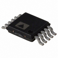
AD5302ARM Analog Devices Inc, AD5302ARM Datasheet - Page 3

AD5302ARM
Manufacturer Part Number
AD5302ARM
Description
IC DAC 8BIT DUAL R-R 10-MSOP
Manufacturer
Analog Devices Inc
Datasheet
1.AD5302ARMZ.pdf
(24 pages)
Specifications of AD5302ARM
Rohs Status
RoHS non-compliant
Settling Time
6µs
Number Of Bits
8
Data Interface
Serial
Number Of Converters
2
Voltage Supply Source
Single Supply
Power Dissipation (max)
2.5mW
Operating Temperature
-40°C ~ 105°C
Mounting Type
Surface Mount
Package / Case
10-MSOP, Micro10™, 10-uMAX, 10-uSOP
Available stocks
Company
Part Number
Manufacturer
Quantity
Price
Company:
Part Number:
AD5302ARM-REEL7
Manufacturer:
AD
Quantity:
5 510
Company:
Part Number:
AD5302ARM-REEL7
Manufacturer:
AD
Quantity:
5 510
Part Number:
AD5302ARMZ
Manufacturer:
ADI/亚德诺
Quantity:
20 000
SPECIFICATIONS
V
Table 1.
Parameter
DC PERFORMANCE
DAC REFERENCE INPUTS
OUTPUT CHARACTERISTICS
LOGIC INPUTS
DD
AD5302
AD5312
AD5322
Offset Error
Gain Error
Lower Deadband
Offset Error Drift
Gain Error Drift
Power Supply Rejection
DC Crosstalk
V
V
Reference Feedthrough
Channel-to-Channel
Minimum Output Voltage
Maximum Output Voltage
DC Output Impedance
Short-Circuit Current
Power-Up Time
Input Current
V
V
Pin Capacitance
REF
REF
IL
IH
Resolution
Relative Accuracy
Differential Nonlinearity
Resolution
Relative Accuracy
Differential Nonlinearity
Resolution
Relative Accuracy
Differential Nonlinearity
Ratio
Isolation
, Input Low Voltage
, Input High Voltage
= 2.5 V to 5.5 V, V
Input Range
Input Impedance
5
2
5
5
5
5
3 , 4
REF
5
5
6
6
= 2 V, R
Min
1
0
2.4
2.1
2.0
L
A Version
= 2 kΩ to GND, C
Typ
8
±0.15
±0.02
10
±0.5
±0.05
12
±2
±0.2
±0.4
±0.15
10
−12
−5
−60
30
>10
180
−90
−80
0.001
V
0.001
0.5
50
20
2.5
5
2
DD
−
1
Max
±1
±0.25
±4
±0.5
±16
±1
±3
±1
60
V
V
±1
0.8
0.6
0.5
3.5
DD
DD
L
Min
1
0
2.4
2.1
2.0
= 200 pF to GND, all specifications T
B Version
Rev. C | Page 3 of 24
±0.02
−12
−5
>10
−80
0.001
2.5
5
Typ
8
±0.15
10
±0.5
±0.05
12
±2
±0.2
±0.4
±0.15
10
−60
30
180
−90
V
0.001
0.5
50
20
2
DD
−
1
Max
±0.5
±0.25
±2
±0.5
±8
±1
±3
±1
60
V
V
±1
0.8
0.6
0.5
3.5
DD
DD
Unit
Bits
LSB
LSB
Bits
LSB
LSB
Bits
LSB
LSB
% of FSR
% of FSR
mV
ppm of
FSR/°C
ppm of
FSR/°C
dB
μV
V
V
MΩ
kΩ
dB
dB
V min
V max
Ω
mA
mA
μs
μs
μA
V
V
V
V
V
V
pF
Test Conditions/Comments
Guaranteed monotonic by design over all codes
Guaranteed monotonic by design over all codes
Guaranteed monotonic by design over all codes
See
See
See
∆V
Buffered reference mode
Unbuffered reference mode
Buffered reference mode
Unbuffered reference mode, input impedance = R
Frequency = 10 kHz
Frequency = 10 kHz
A measure of the minimum drive capability of
the output amplifier
A measure of the maximum drive capability of
the output amplifier
V
V
Coming out of power-down mode, V
Coming out of power-down mode, V
V
V
V
V
V
V
MIN
DD
DD
DD
DD
DD
DD
DD
DD
DD
= 5 V
= 3 V
= 5 V ± 10%
= 3 V ± 10%
= 2.5 V
= 5 V ± 10%
= 3 V ± 10%
= 2.5 V
to T
Figure 3
Figure 3
Figure 3
= ±10%
AD5302/AD5312/AD5322
MAX
, unless otherwise noted.
and
and
and
Figure 4
Figure 4
Figure 4
DD
DD
= 5 V
= 3 V
DAC


