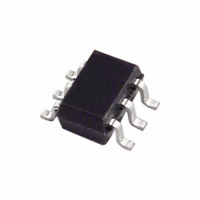
AD5621BKSZ-500RL7 Analog Devices Inc, AD5621BKSZ-500RL7 Datasheet - Page 14

AD5621BKSZ-500RL7
Manufacturer Part Number
AD5621BKSZ-500RL7
Description
IC DAC 12BIT SPI 5V SC70-6
Manufacturer
Analog Devices Inc
Series
nanoDAC™r
Datasheet
1.AD5601BKSZ-REEL7.pdf
(20 pages)
Specifications of AD5621BKSZ-500RL7
Data Interface
SPI™
Settling Time
6µs
Number Of Bits
12
Number Of Converters
1
Voltage Supply Source
Single Supply
Power Dissipation (max)
500µW
Operating Temperature
-40°C ~ 125°C
Mounting Type
Surface Mount
Package / Case
SC-70-6, SC-88, SOT-363
Resolution (bits)
12bit
Sampling Rate
1.7MSPS
Input Channel Type
Serial
Supply Voltage Range - Analog
2.7V To 5.5V
Supply Current
75µA
Digital Ic Case Style
SC-70
Number Of Channels
1
Resolution
12b
Interface Type
Serial (3-Wire, SPI, QSPI, Microwire)
Single Supply Voltage (typ)
3.3/5V
Dual Supply Voltage (typ)
Not RequiredV
Architecture
Resistor-String
Power Supply Requirement
Single
Output Type
Voltage
Integral Nonlinearity Error
±1LSB
Single Supply Voltage (min)
2.7V
Single Supply Voltage (max)
5.5V
Dual Supply Voltage (min)
Not RequiredV
Dual Supply Voltage (max)
Not RequiredV
Operating Temp Range
-40C to 125C
Operating Temperature Classification
Automotive
Mounting
Surface Mount
Pin Count
6
Package Type
SC-70
Lead Free Status / RoHS Status
Lead free / RoHS Compliant
Lead Free Status / RoHS Status
Lead free / RoHS Compliant, Lead free / RoHS Compliant
Available stocks
Company
Part Number
Manufacturer
Quantity
Price
Company:
Part Number:
AD5621BKSZ-500RL7
Manufacturer:
AD
Quantity:
11 650
AD5601/AD5611/AD5621
THEORY OF OPERATION
DAC SECTION
The AD5601/AD5611/AD5621 DACs are fabricated on a
CMOS process. The architecture consists of a string DAC
followed by an output buffer amplifier. Figure 38 is a block
diagram of the DAC architecture.
Because the input coding to the DAC is straight binary, the ideal
output voltage is given by
where:
D is the decimal equivalent of the binary code that is loaded to
the DAC register.
n is the bit resolution of the DAC.
RESISTOR STRING
The resistor string structure is shown in Figure 39. It is simply a
string of resistors, each of Value R. The code loaded to the DAC
register determines at which node on the string the voltage is
tapped off to be fed into the output amplifier. The voltage is
tapped off by closing one of the switches connecting the string
to the amplifier. Because it is a string of resistors, it is guaran-
teed monotonic.
DAC REGISTER
V
OUT
=
V
DD
R
R
R
R
R
Figure 39. Resistor String Structure
×
⎛
⎜
⎝
Figure 38. DAC Architecture
2
D
n
⎞
⎟
⎠
RESISTOR
NETWORK
REF (+)
REF (–)
GND
V
DD
TO OUTPUT
AMPLIFIER
OUTPUT
AMPLIFIER
V
Rev. E | Page 14 of 20
OUT
OUTPUT AMPLIFIER
The output buffer amplifier is capable of generating rail-to-rail
voltages on its output, giving an output range of 0 V to V
capable of driving a load of 2 kΩ in parallel with 1000 pF to
GND. The source and sink capabilities of the output amplifier
are shown in Figure 24. The slew rate is 0.5 V/μs, with a half-
scale settling time of 8 μs with the output loaded.
SERIAL INTERFACE
The AD5601/AD5611/AD5621 have a 3-wire serial interface
( SYNC , SCLK, and SDIN) that is compatible with SPI, QSPI,
and MICROWIRE interface standards as well as most DSPs. See
Figure 2
The write sequence begins by bringing the SYNC line low. Data
from the SDIN line is clocked into the 16-bit shift register on
the falling edge of SCLK. The serial clock frequency can be as
high as 30 MHz, making the AD5601/AD5611/AD5621 com-
patible with high speed DSPs. On the 16
the last data bit is clocked in and the programmed function is
executed (a change in DAC register contents and/or a change
in the mode of operation). At this stage, the SYNC line may be
kept low or brought high. In either case, it must be brought high
for a minimum of 33 ns before the next write sequence so that a
falling edge of SYNC can initiate the next write sequence.
Because the SYNC buffer draws more current when V
than it does when V
between write sequences for even lower power operation of the
part, as mentioned previously. However, it must be brought
high again just before the next write sequence.
INPUT SHIFT REGISTER
The input shift register is 16 bits wide (see Figure 40). The first
two bits are control bits, which control the operating mode of
the part (normal mode or any one of three power-down
modes). For a complete description of the various modes, see
the Power-Down Modes section. For the AD5621, the next
12 bits are the data bits, which are transferred to the DAC
register on the 16
the last two bits is ignored by the AD5621. See Figure 41 and
Figure 42 for the AD5611 and AD5601 input shift register map.
SYNC INTERRUPT
In a normal write sequence, the SYNC line is kept low for at
least 16 falling edges of SCLK and the DAC is updated on the
16
16
The shift register is reset and the write sequence is seen as
invalid. Neither an update of the DAC register contents nor a
change in the operating mode occurs (see
th
th
falling edge. However, if SYNC is brought high before the
falling edge, this acts as an interrupt to the write sequence.
for a timing diagram of a typical write sequence.
th
falling edge of SCLK. The information in
IN
= 0.8 V, SYNC should be idled low
th
falling clock edge,
Figure 43
).
IN
= 1.8 V
DD
. It is


