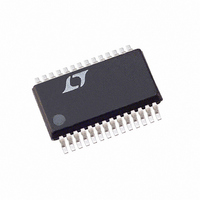
LTC1597ACG#TRPBF Linear Technology, LTC1597ACG#TRPBF Datasheet

LTC1597ACG#TRPBF
Specifications of LTC1597ACG#TRPBF
Available stocks
Related parts for LTC1597ACG#TRPBF
LTC1597ACG#TRPBF Summary of contents
Page 1
... PDIP packages and are specified over the industrial tempera- ture range. For serial interface 16-bit current output DACs refer to the LTC1595/LTC1596 data sheet. , LT, LTC and LTM are registered trademarks of Linear Technology Corporation. All other trademarks are the property of their respective owners. 5V 0.1μF ...
Page 2
LTC1591/LTC1597 ABSOLUTE MAXIMUM V to AGND ............................................... – 0. DGND .............................................. – 0. AGND to DGND ............................................. V DGND to AGND ............................................. V to AGND, DGND .......... ±25V REF, ...
Page 3
ELECTRICAL CHARACTERISTICS = 5V ±10 10V AGND = DGND = 0V REF OUT1 SYMBOL PARAMETER CONDITIONS Accuracy Resolution Monotonicity INL Integral Nonlinearity (Note 2) T DNL Differential Nonlinearity GE Gain Error Unipolar Mode ...
Page 4
LTC1591/LTC1597 ELECTRICAL CHARACTERISTICS = 5V ±10%, V range 10V REF OUT1 SYMBOL PARAMETER Analog Outputs (Note 4) C Output Capacitance (Note 4) OUT Digital Inputs V Digital Input High Voltage IH V Digital Input Low Voltage ...
Page 5
W U TYPICAL PERFOR A CE CHARACTERISTICS Midscale Glitch Impulse 40 USING AN LT1468 C = 30pF 30 FEEDBACK V = 10V REF 1nV-s TYPICAL –10 –20 – 30 – 0.2 0.4 0.6 0.8 1.0 ...
Page 6
LTC1591/LTC1597 W U TYPICAL PERFOR A CE CHARACTERISTICS Integral Nonlinearity (INL) 1.0 0.8 0.6 0.4 0.2 0 – 0.2 – 0.4 – 0.6 – 0.8 –1.0 0 4096 8192 12280 16383 DIGITAL INPUT CODE 1591 G01 Integral Nonlinearity vs Reference ...
Page 7
W U TYPICAL PERFOR A CE CHARACTERISTICS Differential Nonlinearity vs Supply Voltage in Bipolar Mode 1.0 0.8 0.6 0.4 0 2.5V 0 REF – 0.2 – 0.4 – 0.6 – 0.8 –1 SUPPLY VOLTAGE ...
Page 8
LTC1591/LTC1597 W U TYPICAL PERFOR A CE CHARACTERISTICS Integral Nonlinearity (INL) 1.0 0.8 0.6 0.4 0.2 0 – 0.2 – 0.4 – 0.6 – 0.8 –1.0 0 32768 49152 16384 65535 DIGITAL INPUT CODE 1597 G01 Integral Nonlinearity vs Reference ...
Page 9
W U TYPICAL PERFOR A CE CHARACTERISTICS Differential Nonlinearity vs Supply Voltage in Bipolar Mode 1.0 0.8 0.6 0.4 0 2.5V REF – 0 2.5V REF – 0.4 – 0.6 – 0.8 –1 ...
Page 10
LTC1591/LTC1597 PIN FUNCTIONS LTC1591 REF (Pin 1): Reference Input and 4-Quadrant Resistor R2. Typically ±10V, accepts up to ±25V. In 2-Quadrant mode this is the reference input. In 4-quadrant mode, this pin is driven by external inverting ...
Page 11
TRUTH TABLE Table 1 CONTROL INPUTS CLR WR LD REGISTER OPERATION Reset Input and DAC Register to All 0s for LTC1591/LTC1597 and Midscale for LTC1591-1/LTC1597-1 (Asynchronous Operation Load Input Register with All 14/16 Data ...
Page 12
LTC1591/LTC1597 W BLOCK DIAGRA SM REF 1 12k 48k 48k 48k R 2 COM 12k LOAD DIAGRA WR DATA LD CLR 12 LTC1597 48k 48k ...
Page 13
U U APPLICATIONS INFORMATION Description The LTC1591/LTC1597 are 14-/16-bit multiplying, current output DACs with a full parallel 14-/16-bit digital interface. The devices operate from a single 5V supply and provide both unipolar 0V to – 10V 10V ...
Page 14
LTC1591/LTC1597 U U APPLICATIONS INFORMATION 5V 0.1μF V REF REF V R COM CC OFS LTC1597 DATA INPUTS CLR 9 8 ...
Page 15
U U APPLICATIONS INFORMATION V REF + 1/2 LT1112 – REF V COM LTC1591-1 DATA INPUTS 10 TO 21, 24 CLR ...
Page 16
LTC1591/LTC1597 U TYPICAL APPLICATIONS Noninverting Unipolar Operation (2-Quadrant Multiplication COM REF R1 16 DATA INPUTS CLR CLR 0.1μF ...
Page 17
U TYPICAL APPLICATIONS 16-Bit V UNIPOLAR/ BIPOLAR 2 15V LT1236A- DATA INPUTS CLR DAC Programmable Unipolar/Bipolar Configuration OUT LTC203AC LT1468 – ...
Page 18
LTC1591/LTC1597 U TYPICAL APPLICATIONS PHASE ACCUMULATOR n FREQUENCY CONTROL PARALLEL SERIAL SIN ROM DELTA OR BYTE Σ PHASE LOOKUP PHASE LOAD REGISTER REGISTER REGISTER M CLOCK PHASE BITS TRUNCATION 16 BITS ...
Page 19
... MOLD FLASH OR PROTRUSIONS SHALL NOT EXCEED 0.010 INCH (0.254mm) Information furnished by Linear Technology Corporation is believed to be accurate and reliable. However, no responsibility is assumed for its use. Linear Technology Corporation makes no represen- tation that the interconnection of its circuits as described herein will not infringe on existing patent rights. ...
Page 20
... Low Noise and Glitch Rail-to-Rail VOUT Low Power, 8-Lead MSOP Rail-to-Rail VOUT 16mW Dissipation, Serial and Parallel Outputs ±2.5V Input, SINAD = 90dB, THD = 100dB Low Power, ±10V Inputs Ultralow Drift, 5ppm/°C, High Accuracy 0.05% LT 0507 REV A • PRINTED IN USA © LINEAR TECHNOLOGY CORPORATION 1998 15917fa ...


