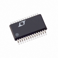
LTC1597ACG#TR Linear Technology, LTC1597ACG#TR Datasheet - Page 10

LTC1597ACG#TR
Manufacturer Part Number
LTC1597ACG#TR
Description
IC DAC 14BIT PARALLEL IN 28SSOP
Manufacturer
Linear Technology
Datasheet
1.LTC1591CGPBF.pdf
(20 pages)
Specifications of LTC1597ACG#TR
Settling Time
1µs
Number Of Bits
16
Data Interface
Parallel
Number Of Converters
1
Voltage Supply Source
Single Supply
Power Dissipation (max)
55µW
Operating Temperature
0°C ~ 70°C
Mounting Type
Surface Mount
Package / Case
28-SSOP
Lead Free Status / RoHS Status
Contains lead / RoHS non-compliant
Available stocks
Company
Part Number
Manufacturer
Quantity
Price
LTC1591/LTC1597
LTC1591
REF (Pin 1): Reference Input and 4-Quadrant Resistor R2.
Typically ±10V, accepts up to ±25V. In 2-Quadrant mode
this is the reference input. In 4-quadrant mode, this pin is
driven by external inverting reference amplifier.
R
Resistors R1 and R2. Normally tied to the inverting input
of an external amplifier in 4-quadrant operation, otherwise
shorted to the REF pin. See Figures 1a and 2a.
R1 (Pin 3): 4-Quadrant Resistor R1. In 2-quadrant opera-
tion short to the REF pin. In 4-quadrant mode tie to R
(Pin 4).
R
±10V, accepts up to ±25V. In 2-quadrant operation tie to
R
R
of the current to voltage converter op amp. Swings to
±V
LTC1597
REF (Pin 1): Reference Input and 4-Quadrant Resistor R2.
Typically ±10V, accepts up to ±25V. In 2-Quadrant mode
this is the reference input. In 4-quadrant mode, this pin is
driven by external inverting reference amplifier.
R
Resistors R1 and R2. Normally tied to the inverting input
of an external amplifier in 4-quadrant operation, otherwise
shorted to the REF pin. See Figures 1b and 2b.
R1 (Pin 3): 4-Quadrant Resistor R1. In 2-quadrant opera-
tion short to the REF pin. In 4-quadrant mode tie to R
(Pin 4).
R
±10V, accepts up to ±25V. In 2-quadrant operation tie to
R
R
of the current to voltage converter op amp. Swings to
±V
10
PIN
COM
OFS
FB
FB
COM
OFS
FB
FB
REF
REF
U
. In 4-quadrant operation tie to R1.
. In 4-quadrant operation tie to R1.
(Pin 5): Feedback Resistor. Normally tied to the output
(Pin 5): Feedback Resistor. Normally tied to the output
(Pin 4): Bipolar Offset Resistor. Typically swings
(Pin 4): Bipolar Offset Resistor. Typically swings
. V
. V
(Pin 2): Center Tap Point of the Two 4-Quadrant
(Pin 2): Center Tap Point of the Two 4-Quadrant
FUNCTIONS
REF
REF
U
is typically ±10V.
is typically ±10V.
U
OFS
OFS
I
input of the current to voltage converter op amp.
AGND (Pin 7): Analog Ground. Tie to ground.
LD (Pin 8): DAC Digital Input Load Control Input. When LD
is taken to a logic high, data is loaded from the input
register into the DAC register, updating the DAC output.
WR (Pin 9):DAC Digital Write Control Input. When WR is
taken to a logic low, data is loaded from the digital input
pins into the 14-bit wide input register.
DB13 to D2 (Pins 10 to 21): Digital Input Data Bits.
DGND (Pin 22): Digital Ground. Tie to ground.
V
Requires a bypass capacitor to ground.
DB1, DB0 (Pins 24, 25): Digital Input Data Bits.
NC (Pins 26, 27): No Connect.
CLR (Pin 28):Digital Clear Control Function for the DAC.
When CLR is taken to a logic low, it sets the DAC output
and all internal registers to zero code for the LTC1591 and
midscale code for the LTC1591-1.
I
input of the current to voltage converter op amp.
AGND (Pin 7): Analog Ground. Tie to ground.
LD (Pin 8): DAC Digital Input Load Control Input. When LD
is taken to a logic high, data is loaded from the input
register into the DAC register, updating the DAC output.
WR (Pin 9):DAC Digital Write Control Input. When WR is
taken to a logic low, data is loaded from the digital input
pins into the 16-bit wide input register.
DB15 to D4 (Pins 10 to 21): Digital Input Data Bits.
DGND (Pin 22): Digital Ground. Tie to ground.
V
Requires a bypass capacitor to ground.
DB3 to DB0 (Pins 24 to 27): Digital Input Data Bits.
CLR (Pin 28):Digital Clear Control Function for the DAC.
When CLR is taken to a logic low, it sets the DAC output
and all internal registers to zero code for the LTC1597 and
midscale code for the LTC1597-1.
OUT1
OUT1
CC
CC
(Pin 23): The Positive Supply Input. 4.5V ≤ V
(Pin 23): The Positive Supply Input. 4.5V ≤ V
(Pin 6): DAC Current Output. Tie to the inverting
(Pin 6): DAC Current Output. Tie to the inverting
CC
CC
≥ 5.5V.
≥ 5.5V.
15917fa


