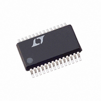
LTC1458IG#PBF Linear Technology, LTC1458IG#PBF Datasheet - Page 7

LTC1458IG#PBF
Manufacturer Part Number
LTC1458IG#PBF
Description
IC D/A CONV 12BIT R-R QUAD28SSOP
Manufacturer
Linear Technology
Datasheet
1.LTC1458CSWPBF.pdf
(12 pages)
Specifications of LTC1458IG#PBF
Settling Time
14µs
Number Of Bits
12
Data Interface
Serial
Number Of Converters
4
Voltage Supply Source
Single Supply
Power Dissipation (max)
5.5mW
Operating Temperature
-40°C ~ 85°C
Mounting Type
Surface Mount
Package / Case
28-SSOP
Number Of Channels
4
Resolution
12b
Interface Type
Serial (3-Wire)
Single Supply Voltage (typ)
5V
Dual Supply Voltage (typ)
Not RequiredV
Power Supply Requirement
Single
Output Type
Voltage
Single Supply Voltage (min)
4.5V
Single Supply Voltage (max)
5.5V
Dual Supply Voltage (min)
Not RequiredV
Dual Supply Voltage (max)
Not RequiredV
Operating Temp Range
-40C to 85C
Operating Temperature Classification
Industrial
Mounting
Surface Mount
Pin Count
28
Lead Free Status / RoHS Status
Lead free / RoHS Compliant
Available stocks
Company
Part Number
Manufacturer
Quantity
Price
DEFI ITIO S
TI I G DIAGRA
Resolution (n): Resolution is defined as the number of
digital input bits, n. It defines the number of DAC output
states (2
does not imply linearity.
Full-Scale Voltage (V
when all bits are set to 1.
Voltage Offset Error (V
output when the DAC is loaded with all zeros. The output
amplifier can have a true negative offset, but because the
part is operated from a single supply, the output cannot go
below zero. If the offset is negative, the output will remain
near 0V resulting in the transfer curve shown in Figure 1.
CS/LD
D
CLK
OUT
D
W
IN
U
U
NEGATIVE
PREVIOUS WORD
n
) that divide the full-scale range. The resolution
OFFSET
VOLTAGE
OUTPUT
B0 D
Figure 1. Effect of Negative Offset
U
0V
PREVIOUS WORD
t
9
B11 A
FS
OS
): This is the output of the DAC
): The theoretical voltage at the
DAC CODE
W
B11 A
MSB
PREVIOUS WORD
B10 A
t
4
1458 F01
PREVIOUS WORD
B0 B
t
B0 B
8
LSB
t
3
The offset of the part is measured at the code that corre-
sponds to the maximum offset specification:
Least Significant Bit (LSB): One LSB is the ideal voltage
difference between two successive codes.
Nominal LSBs:
Integral Nonlinearity (INL): End-point INL is the maxi-
mum deviation from a straight line passing through the
end-points of the DAC transfer curve. Because the part
operates from a single supply and the output cannot go
below zero, the linearity is measured between full scale
and the code corresponding to the maximum offset
specification. The INL error at a given input code is
calculated as follows:
PREVIOUS WORD
V
LSB = (V
LTC1458
LTC1458L
INL
V
OS
OUT
B11 C
= V
t
1
= [V
= The output voltage of the DAC measured at
OUT
B11 C
MSB
FS
the given input code
t
– V
OUT
2
– [(Code)(V
LSB = 4.095V/4095 = 1mV
LSB = 2.5V/4095 = 0.610mV
OS
– V
)/(2
OS
LTC1458/LTC1458L
n
– (V
– 1) = (V
FS
PREVIOUS WORD
)/(2
FS
– V
B0 D
n
– 1)]
FS
OS
B0 D
LSB
– V
t
)(code/4095)]/LSB
6
OS
)/4095
t
5
CURRENT WORD
B11 A
t
7
7
1458 TD


