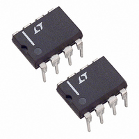
LTC1655IN8 Linear Technology, LTC1655IN8 Datasheet

LTC1655IN8
Specifications of LTC1655IN8
Available stocks
Related parts for LTC1655IN8
LTC1655IN8 Summary of contents
Page 1
... The LTC1655/LTC1655L are pin compatible with Linear Technology’s 12-bit V upgrade path. They are the only buffered 16-bit DACs in an SO-8 package and they include an onboard reference for standalone performance. , LTC and LT are registered trademarks of Linear Technology Corporation. MICROWIRE is a trademark of National Semiconductor Corporation REF ...
Page 2
... LTC1655, REF = 2.2V (Note 8) (External) CC LTC1655L, REF = 1.3V 2.7V (Note 8) (External) CC REF = 2.2V (External (Note 8) CC For Specified Performance LTC1655 LTC1655L (Note ORDER PART NUMBER TOP VIEW LTC1655CN8 LTC1655IN8 LTC1655CS8 7 V OUT LTC1655IS8 REF 6 LTC1655LCN8 5 GND LTC1655LIN8 S8 PACKAGE LTC1655LCS8 8-LEAD PLASTIC SO LTC1655LIS8 ...
Page 3
ELECTRICAL CHARACTERISTICS The denotes specifications which apply over the full operating temperature range, otherwise specifications are 4.5V to 5.5V (LTC1655 2.7V to 5.5V (LTC1655L SYMBOL PARAMETER Op Amp DC Performance Short-Circuit ...
Page 4
LTC1655/LTC1655L ELECTRICAL CHARACTERISTICS The denotes specifications which apply over the full operating temperature range, otherwise specifications are 4.5V to 5.5V (LTC1655 2.7V to 5.5V (LTC1655L SYMBOL PARAMETER I Digital Input Leakage ...
Page 5
W U TYPICAL PERFORMANCE CHARACTERISTICS (LTC1655 (LTC1655L) unless otherwise noted TC1655 Differential Nonlinearity 1.0 0.8 0.6 0.4 0.2 0 –0.2 –0.4 –0.6 –0.8 –1.0 0 16,384 32,768 DIGITAL INPUT CODE LTC1655 Integral ...
Page 6
LTC1655/LTC1655L W U TYPICAL PERFORMANCE CHARACTERISTICS (LTC1655 (LTC1655L) unless otherwise noted LTC1655 Minimum Output Voltage vs Output Sink Current 1.0 CODE: ALL 0s 0.8 0.6 125 C 0 0.2 0 ...
Page 7
W U TYPICAL PERFORMANCE CHARACTERISTICS (LTC1655 (LTC1655L) unless otherwise noted LTC1655 Supply Current vs Logic Input Voltage 3.0 2.6 2.2 1.8 1.4 1.0 0 LOGIC INPUT VOLTAGE (V) ...
Page 8
LTC1655/LTC1655L PIN FUNCTIONS CLK (Pin 1): The TTL Level Input for the Serial Interface Clock. D (Pin 2): The TTL Level Input for the Serial Interface IN Data. Data on the D pin is latched into the ...
Page 9
U U DEFI ITIO S Differential Nonlinearity (DNL): The difference between the measured change and the ideal 1LSB change for any two adjacent codes. The DNL error between any two codes is calculated as follows: DNL = ( V – ...
Page 10
LTC1655/LTC1655L U U APPLICATIONS INFORMATION Rail-to-Rail Output Considerations In any rail-to-rail DAC, the output swing is limited to voltages within the supply range. If the DAC offset is negative, the output for the lowest codes limits shown ...
Page 11
U TYPICAL APPLICATIONS This circuit shows how to use an LTC1655 to make an optoisolated digitally controlled 4mA to 20mA process controller. The controller circuitry, including the optoisolation, is powered by the loop voltage that can have a wide range ...
Page 12
LTC1655/LTC1655L U TYPICAL APPLICATIONS This circuit shows how to make a bipolar output 16-bit DAC with a wide output swing using an LTC1655 and an LT1077. R1 and R2 resistively divide down the LTC1655 output and an offset is summed ...
Page 13
U TYPICAL APPLICATIONS This circuit shows a digitally programmable current source from an external voltage source using an external op amp, an LT1218 and an NPN transistor (2N3440). Any digital word from 0 to 65535 is loaded into the LTC1655 ...
Page 14
LTC1655/LTC1655L PACKAGE DESCRIPTION 0.300 – 0.325 (7.620 – 8.255) 0.009 – 0.015 (0.229 – 0.381) +0.035 0.325 –0.015 +0.889 8.255 –0.381 *THESE DIMENSIONS DO NOT INCLUDE MOLD FLASH OR PROTRUSIONS. MOLD FLASH OR PROTRUSIONS SHALL NOT EXCEED 0.010 INCH (0.254mm) ...
Page 15
... FLASH SHALL NOT EXCEED 0.010" (0.254mm) PER SIDE Information furnished by Linear Technology Corporation is believed to be accurate and reliable. However, no responsibility is assumed for its use. Linear Technology Corporation makes no represen- tation that the interconnection of its circuits as described herein will not infringe on existing patent rights. ...
Page 16
... OUT = 4.5V to 5.5V 4.095V CC OUT = 2.7V to 5.5V 2.5V CC OUT DAC, OUT = 5V, Low Power, Deglitched 4.096V CC OUT = 3V, Low Power, Deglitched 2.5V CC OUT DAC in MS8 Package. Output OUT CC DAC in MS8 Package. Output OUT CC 16555lf LT/TP 0800 4K • PRINTED IN USA LINEAR TECHNOLOGY CORPORATION 1998 CC ...


